
High sensitivity magnetic built-in current sensor

a built-in current sensor, high-sensitivity technology, applied in the field of current sensors, can solve the problems of narrowing the difference between the iddq level of a fault-free and a faulty circuit, and not being sufficiently sensitive, and achieve the effect of increasing the sensitivity of the sensor

Inactive Publication Date: 2009-11-17
ELIPOSKI REMOTE
View PDF13 Cites 115 Cited by
  • Summary
  • Abstract
  • Description
  • Claims
  • Application Information

AI Technical Summary

Benefits of technology

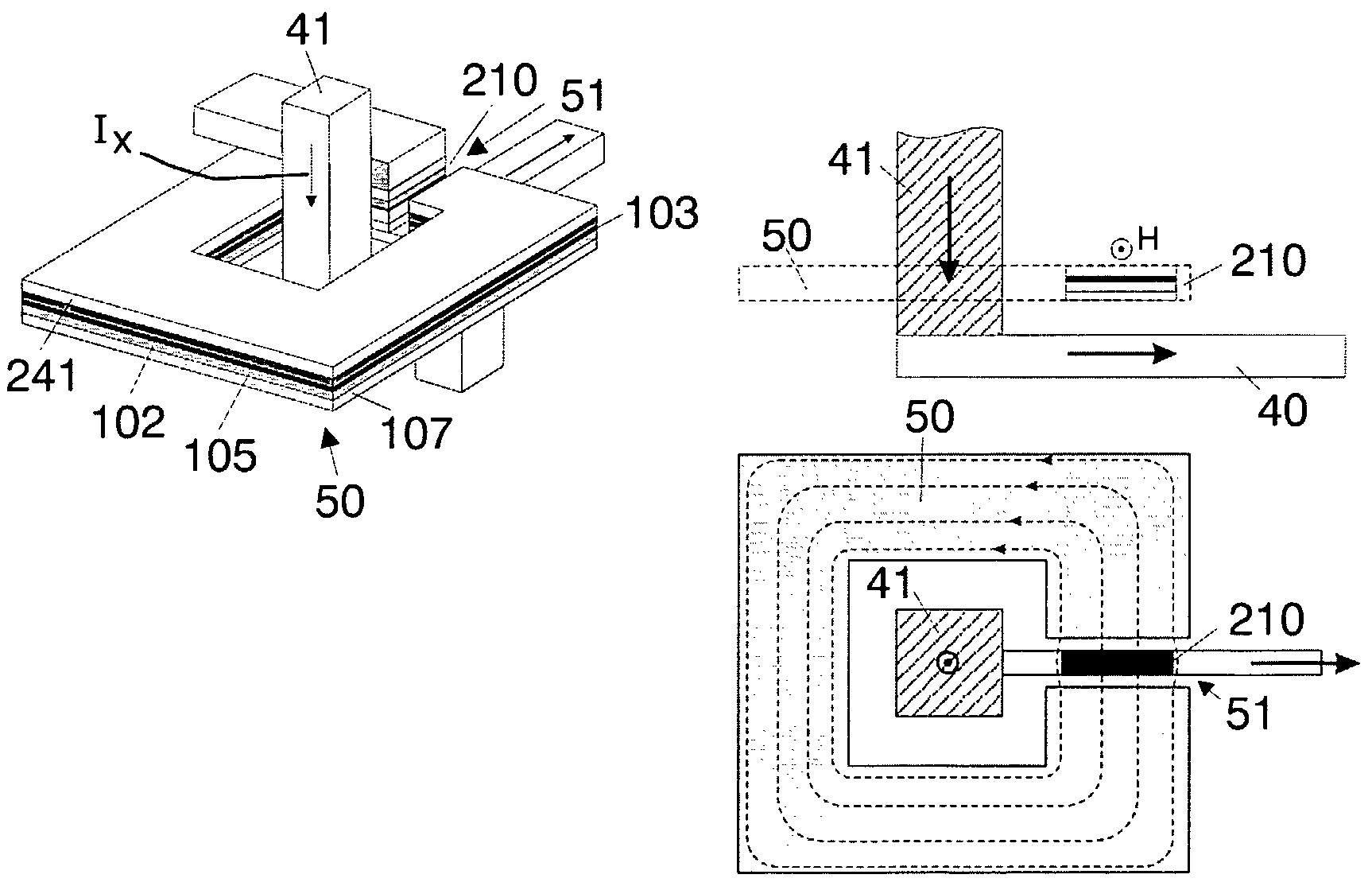
[0010]In a first aspect, the present invention provides a semiconductor device with a conductive element and a current sensor. The current sensor is a magnetic current sensing device for sensing direct, varying or alternating current flowing through the conductive element. The current sensing device is integrated in the semiconductor device and is galvanically isolated from the conductive element. An advantage is greater sensitivity of the sensor compared to prior art sensors: the sensor may be suitable for measuring current with a μA resolution. The greater sensitivity enables less signal post processing and electronic circuitry to be used, which is important for applications such as mobile devices. Notably sufficient sensitivity can be obtained in principle for IDD measurements such as quiescent IDD current (IDDQ) or transient IDD current (IDDT), even for next generation CMOS processes which have more stringent IDD test requirements. IDDQ is the quiescent current flowing from Vdd to Vss (IDD current) in CMOS circuitry, in a quiescent state. IDDT is the transient IDD current during digital transitions. Measuring the IDDQ and IDDT currents allow to detect faults within the CMOS circuitry.
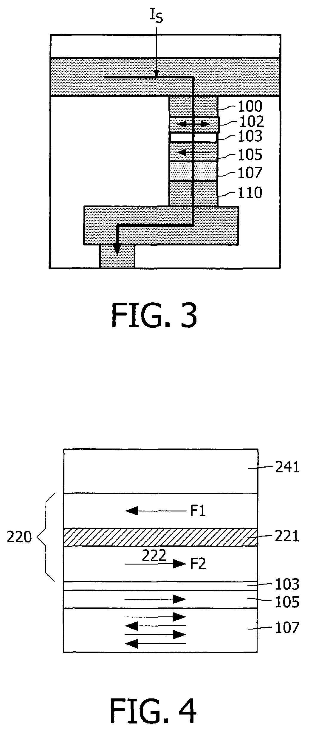
[0043]If the free region has a net magnetic moment which is substantially zero, a method according to the present invention includes modifying the net magnetic moment of the free region so as to make it non-zero. This increases the sensitivity of a sensor of the toggle type. Modifying the net magnetic moment may comprise increasing or decreasing the magnetic moment of at least one of the ferromagnetic layers in the free magnetic regions, e.g. by at least partially removing or destroying one of the ferromagnetic layers of the free magnetic region, or locally converting the anti-ferromagnetic coupling into a ferromagnetic coupling.

Problems solved by technology

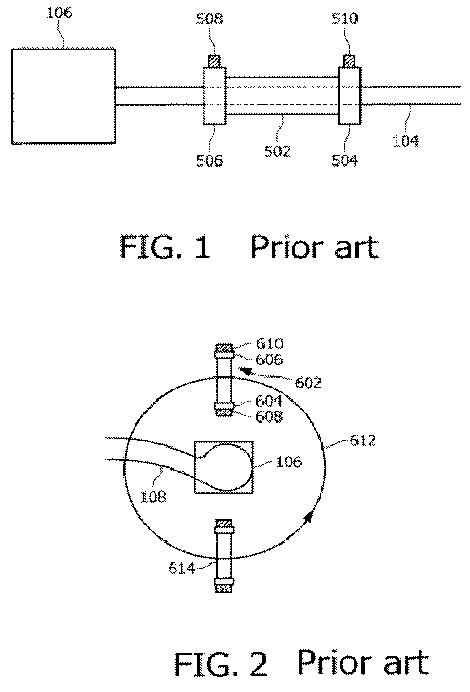
Such sensors are useful for sensing high currents, but are not sufficiently sensitive for applications such as Quiescent Current (IDDQ) testing.
However MOSFET leakage currents are rising rapidly with each technology node, narrowing the difference between the IDDQ levels of a faulty and fault-free circuit.

Method used


Image

  • High sensitivity magnetic built-in current sensor
  • High sensitivity magnetic built-in current sensor
  • High sensitivity magnetic built-in current sensor

Examples


Embodiment Construction

[0076]The present invention will be described with respect to particular embodiments and with reference to certain drawings but the invention is not limited thereto but only by the claims. The drawings described are only schematic and are non-limiting. In the drawings, the size of some of the elements may be exaggerated and not drawn on scale for illustrative purposes. Where the term “comprising” is used in the present description and claims, it does not exclude other elements or steps. Where an indefinite or definite article is used when referring to a singular noun e.g. “a” or “an”, “the”, this includes a plural of that noun unless something else is specifically stated.

[0077]By way of introduction to the description of embodiments of the invention, MRAM development will be explained briefly. During recent years, research into Magnetic RAM (MRAM) has been intense. The integration of magnetic materials with CMOS technology has become less of a problem. Commercial MRAM production is ...


PUM


Abstract

A sensor for contactlessly detecting currents, has a sensor element having a magnetic tunnel junction (MTJ), and detection circuitry, the sensor element having a resistance which varies with the magnetic field, and the detection circuitry is arranged to detect a tunnel current flowing through the tunnel junction. The sensor element may share an MTJ stack with memory elements. Also it can provide easy integration with next generation CMOS processes, including MRAM technology, be more compact, and use less power. Solutions for increasing sensitivity of the sensor, such as providing a flux concentrator, and for generating higher magnetic fields with a same current, such as forming L-shaped conductor elements, are given. The greater sensitivity enables less post processing to be used, to save power for applications such as mobile devices. Applications include current sensors, built-in current sensors, and IDDQ and IDDT testing, even for next generation CMOS processes.

Description

CROSS-REFERENCE TO RELATED APPLICATIONS[0001]This application is a 371 of PCT / 1B04 / 52857 filed on Dec. 20, 2004, the entirely of which is hereby incorporated by reference herein.FIELD OF THE INVENTION[0002]This invention relates to current sensors for sensing of current in a conductor, to integrated circuits having such a sensor built-in, to methods of using such sensors, and to methods for sensing current in a conductor in a semiconductor device such as an integrated circuit, amongst others as well as software products for implementing the methods of use.BACKGROUND OF THE INVENTION[0003]There are various types of known BICS (Built In Current Sensor). Some are described in U.S. Pat. No. 5,963,038, which shows detecting faults in integrated circuits by measurement of current through a conductor in the integrated circuit by means of a sensor situated in the vicinity of the conductor. The sensor can be constructed in various ways so as to measure the field produced by the current throu...

Claims


Application Information

Patent Timeline
IPC IPC(8): G01R31/26G11C11/00G01R15/20G01R31/30G01R33/09G11C11/15G11C11/16
CPCG01R15/20G11C11/16G01R31/3004G11C11/1673G11C11/1675G01R31/30G01R33/09
Inventor DE WILDE, JOHANNESPINEDA DE GYVEZ, JOSE DE JESUSDE JONG, FRANCISCUS GERARDUS MARIAHUISKEN, JOSEPHUS ANTONIUSBOEVE, HANS MARC BERTPHAN LE, KIM
Owner ELIPOSKI REMOTE
Learn More