Method for manufacturing display device

a display device and manufacturing method technology, applied in non-linear optics, instruments, coatings, etc., can solve the problem of requiring additional cost, and achieve the effect of reducing the waste of materials used in manufacturing a display device, reducing manufacturing costs, and simplifying the process

Inactive Publication Date: 2009-12-01
SEMICON ENERGY LAB CO LTD
View PDF111 Cites 14 Cited by
  • Summary
  • Abstract
  • Description
  • Claims
  • Application Information

AI Technical Summary

Benefits of technology

[0013]By manufacturing a display device by using a manufacturing method of a display device of the invention, a waste of the material used for manufacturing a display device can be reduced. Therefore, manufacturing cost can be reduced. By manufacturing a display device by using a manufacturing method of a display device of the invention, simplification of the process, device and a manufacturing line of smaller scale, and a shorter time for the process can be achieved. Further, an impact on the environment can be reduced since energy can be reduced as the equipment of the exhaust system which was conventionally required can be simplified.

Problems solved by technology

In order to provide this equipment, a space is required for the exhaust system externally the processing apparatus, which requires additional cost.

Method used


Image

  • Method for manufacturing display device
  • Method for manufacturing display device
  • Method for manufacturing display device

Examples


embodiment mode 1

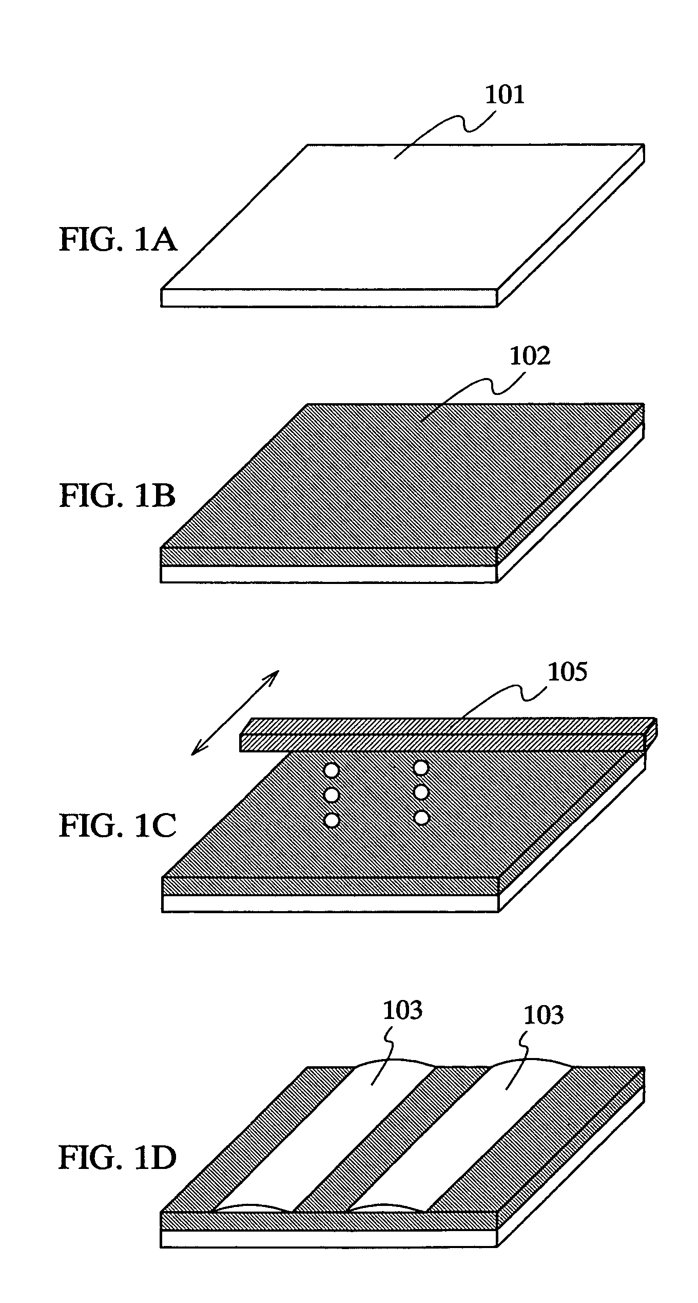
[0034]In this embodiment mode, a wiring pattern which is essential for a display device is formed on a glass substrate of a desired size by using a liquid droplet ejecting apparatus having a liquid droplet ejecting head provided with a plurality of liquid droplet ejecting nozzles arranged linearly and a plasma processing apparatus having a plasma generating means at an atmospheric pressure or a pressure close to the atmospheric pressure. In particular, the invention is intended to be applied to a substrate of the fifth generation or after thereof which is larger in size. Embodiment Mode 1 of the invention is hereafter described with reference to the drawings.

[0035]First, a conductive film 102 which is to be a wiring is deposited (FIG. 1B) on a substrate 101 being processed which is formed of various materials such as glass, quartz, a semiconductor, plastic, a plastic film, metal, glass epoxy resin, ceramic by using a known method such as sputtering or a CVD method (Chemical Vapor De...

embodiment mode 2

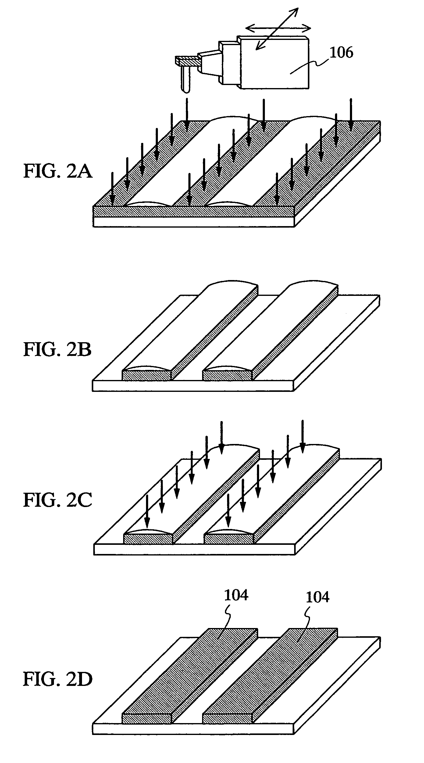
[0066]This embodiment mode is characterized in that a wiring is formed by using only a linear liquid droplet ejecting apparatus having a liquid droplet ejecting head provided with a plurality of liquid droplet ejecting orifices.

[0067]A material containing conductive ultrafine particles is ejected from the linear liquid droplet ejecting apparatus to a glass substrate 801. At this time, by scanning a head 802 which ejects liquid droplets or the glass substrate 801, a wiring pattern is formed (FIG. 8B). By processing the glass substrate 801 with heat on which the wiring pattern is formed, a wiring 804 is formed (FIG. 8C).

[0068]Here, a diameter of a nozzle used for the liquid droplet ejecting means described above is set 0.1 to 50 μm (more preferably 0.6 to 26 μm) and an ejecting amount of a compound ejected from the nozzle is set 0.00001 pl to 50 pl (more preferably 0.0001 to 40 pl). This ejecting amount increases in proportion to a size of the diameter of the nozzle. A distance betwee...

embodiment mode 3

[0072]This embodiment mode is characterized in that the plasma processing apparatus only is used to form a wiring. Hereafter, this embodiment mode is described.

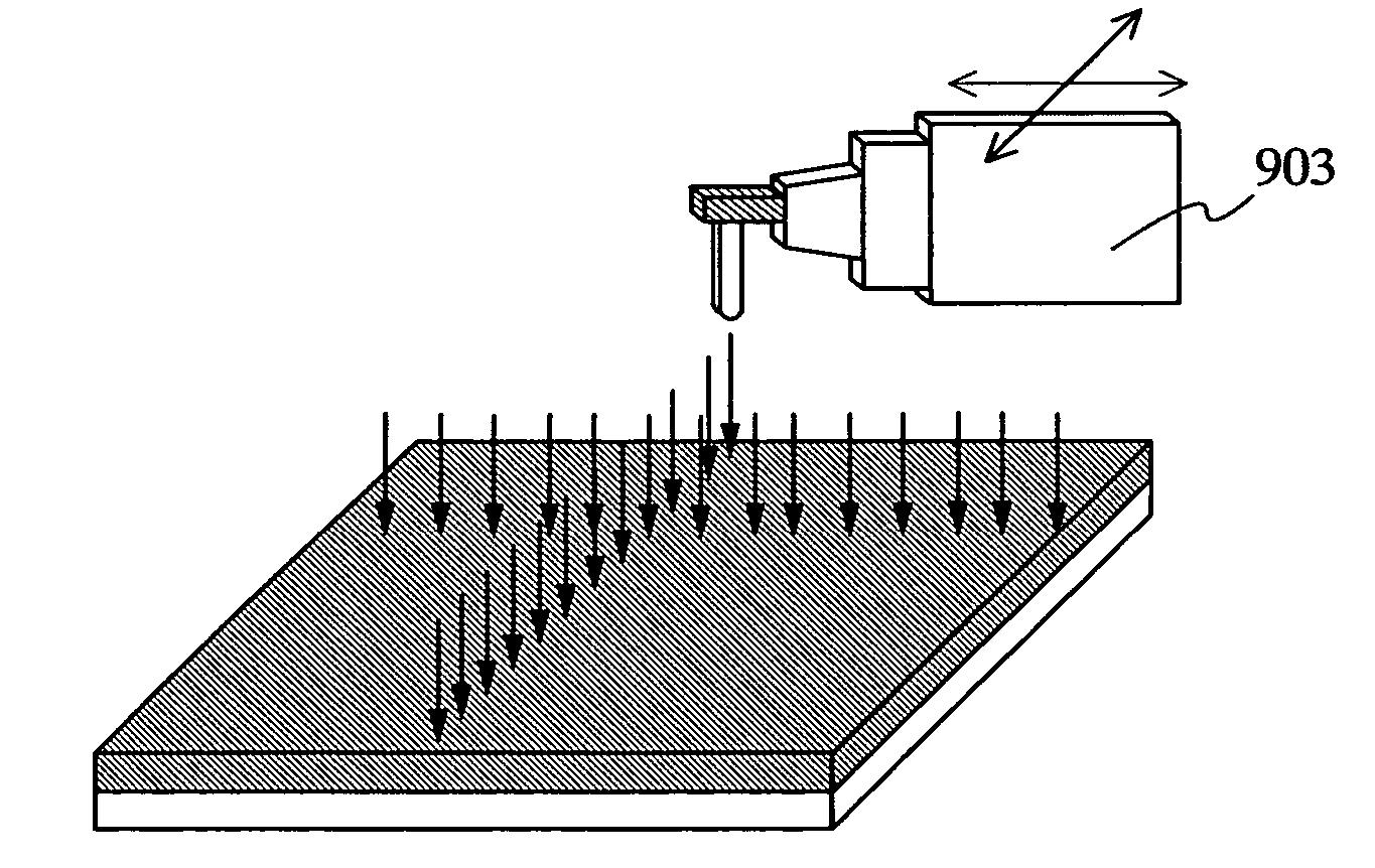
[0073]First, a conductive film 902 which is to be a wiring is formed on a substrate 901 being processed by using a sputter processing method (FIGS. 9A and 9B). Next, the conductive film 902 is selectively etched in an atmospheric pressure or a pressure close to the atmospheric pressure by using the plasma processing apparatus having the plasma generating means provided with a pair of cylindrical electrodes or having a plasma generating means having a plurality of pairs of cylindrical electrodes arranged linearly which are also used in Embodiment Mode 1 (FIG. 9C). The etching is performed by scanning the substrate 901 being processed in one direction (or the plasma generating means 903 in one direction) so that a portion required to be removed only is selectively etched in the conductive film 902.

[0074]As described above, the ...


PUM

PropertyMeasurementUnit
sizeaaaaaaaaaa
pressureaaaaaaaaaa
distanceaaaaaaaaaa

Abstract

In order to achieve low cost of manufacture of a display device by reducing the use of primary material used in a manufacturing process of a display device and saving labor taken for a vacuum process, according to the invention, liquid droplets containing conductive particles are ejected on a film being processed by using a first liquid droplet ejecting apparatus having a liquid droplet ejecting head provided with a plurality of liquid droplet ejecting orifices, thereby a conductive film is formed. After that, a resist pattern is locally formed on the conductive film by using a second liquid droplet ejecting apparatus having a liquid droplet ejecting head provided with a plurality of liquid droplet ejecting orifices. The conductive film is etched with the resist pattern as a mask to form a wiring.

Description

TECHNICAL FIELD[0001]The present invention relates to a manufacturing method of a display device represented by a liquid crystal display device (LCD).BACKGROUND ART[0002]Conventionally, a thin film transistor (TFT) included in a display device represented by a liquid crystal display device (LCD) and a self-luminous display device (EL: Electroluminescence) display device) has been formed by a vacuum process that the interior of a processing apparatus is in reduced pressure or in vacuum, or by a photolithography process that a mask of (photo) resist is formed by an exposure apparatus and unnecessary portions are removed by etching.[0003]The vacuum process requires a process chamber used for depositing a film on a substrate being processed, performing etching and the like, and an exhaust means for making a vacuum state or a reduced pressure state.[0004]The exhaust means is formed of a pump represented by a turbo molecular pump, rotary pump and the like provided externally the processin...

Claims


Application Information

Patent Timeline
Patent Type & Authority Patents(United States)
IPC IPC(8): B05D5/12G02F1/1343G02F1/1362H01L21/288H01L21/3213H01L21/336H01L21/768H01L27/32H01L29/786H01L51/00H01L51/40H01L51/56
CPCG02F1/13439H01L21/288H01L21/32136H01L21/32139H01L21/76838H01L51/56H01L29/66765H01L29/78669H01L51/0021H01L51/0022G02F2001/136295H01L51/0005H01L51/0023H01L27/3244G02F1/136295H10K59/12H10K71/135H10K71/60H10K71/611H10K71/621H10K71/00G02F1/136
Inventor YAMAZAKI, SHUNPEI
Owner SEMICON ENERGY LAB CO LTD
Why Eureka
Try Eureka