A/D converter circuit and A/D conversion method

a converter circuit and converter technology, applied in the field of a/d converter circuit and a/d conversion method, can solve the problems of increasing the scale of the arithmetic processing circuit, requiring an extended period of time for the complicated operation, and the technology is not suited to high-speed a/d conversion processing, so as to suppress the variation of digital data

Active Publication Date: 2009-12-29
DENSO CORP
View PDF14 Cites 9 Cited by
  • Summary
  • Abstract
  • Description
  • Claims
  • Application Information

AI Technical Summary

Benefits of technology

[0008]It is therefore an object of the present invention to provide an A / D converter circuit and an A / D conversion method capable of suppressing variation in digital data caused by a change in ambient temperature without requiring complicated arithmetic processing.

Problems solved by technology

Therefore, even if a variation in the digital data caused by the ambient temperature can be suppressed, the scale of the arithmetic processing circuit increases and, besides, an extended period of time is required for the complicated operation that occurs repetitively.
Thus, this technology is not suited for high-speed A / D conversion processing.
However, the cost of the GaAs device itself and the presence of the pulse circulating circuit that does not require high-speed processing necessitate a new step in the process for producing the semiconductors and increases costs of production.

Method used


Image

  • A/D converter circuit and A/D conversion method
  • A/D converter circuit and A/D conversion method
  • A/D converter circuit and A/D conversion method

Examples


first embodiment

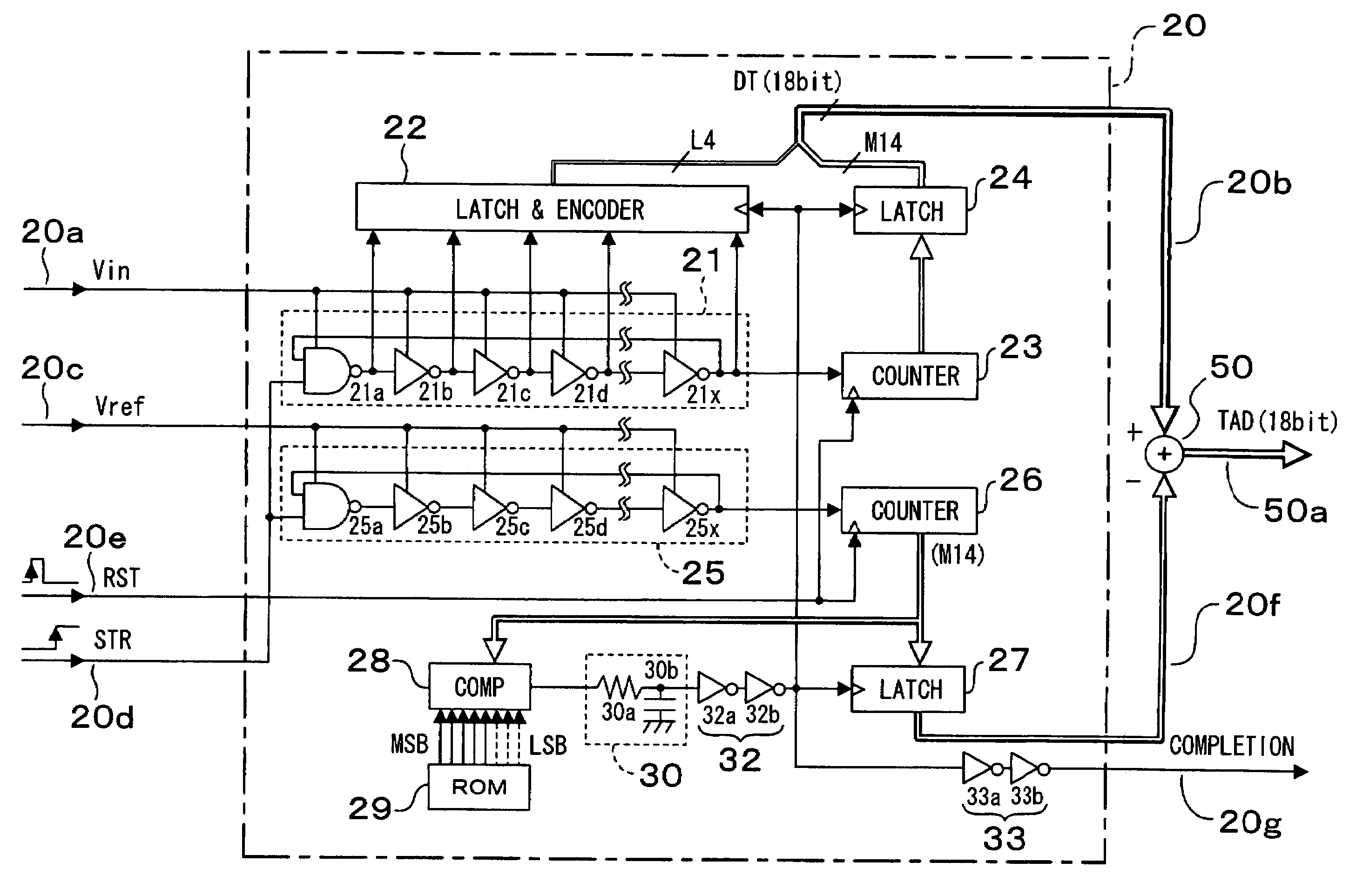
[0036]Referring to FIG. 1, an A / D converter circuit 20 is provided for converting an analog input voltage Vin input to an input line 20a into a binary digital data DT and for outputting it to an output line 20b, and is formed by a first ring delay line 21, a latch and encoder 22, a first counter 23, a first latch 24, a second ring delay line 25, a second counter 26, a second latch 27, a digital comparator 28, a ROM 29, a low-pass filter (LPF) 30, and output buffers 32 and 33 and the like. The A / D converter circuit 20, as will be described below, utilizes the fact that the inverting operation time of the inverting circuits in the first ring delay line 21 differs depending upon the input voltage Vin.

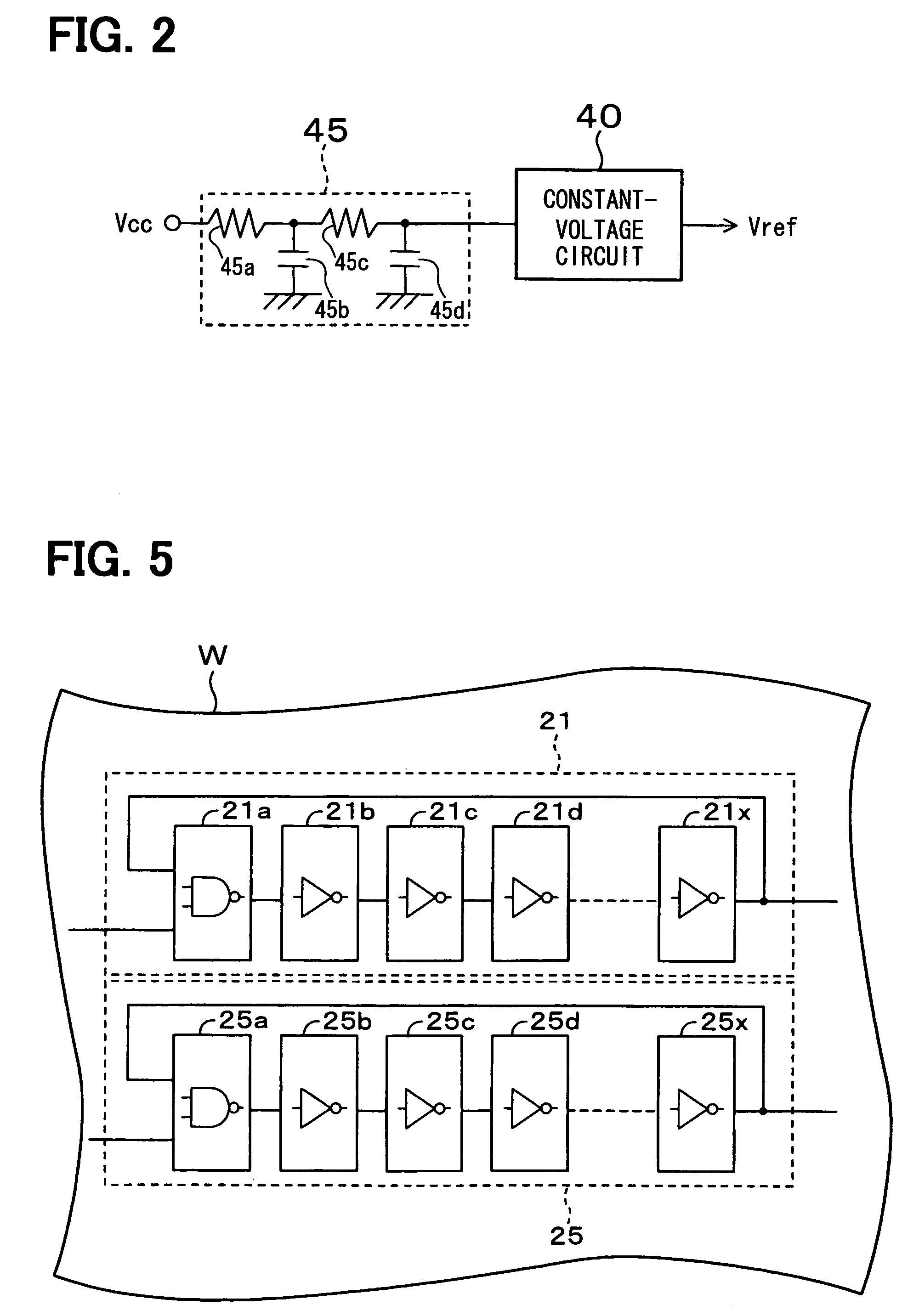
[0037]The first ring delay line 21 is formed by coupling a plurality of inverting circuits 21a, 21b, 21c, 21d to 21x in a ring form, the plurality of inverting circuits using the input voltage Vin input from the input line 20a as a power supply voltage and of which the inverting operation ...

second embodiment

[0090]An A / D converter circuit 120 according to a second embodiment is shown in FIG. 8. The A / D converter circuit 120 is different from the A / D converter circuit 20 with respect to that the configuration of the digital comparator 28 is varied and the LPF 30 is omitted. Therefore, the constituent portions substantially the same as those of the A / D converter circuit 20 of the first embodiment are denoted by the same reference numerals.

[0091]The A / D converter circuit 120 is formed without providing the LPF 30 between the digital comparator 128 and the second latch 27. That is, as shown in FIG. 9, a delay circuit 128al, an EXOR circuit 128b1, a flip-flop circuit 128a3, etc. are provided as compared to the digital comparator 28 of the first embodiment shown in FIG. 3. That is, despite the glitch noise, if the counter value output from the second counter 26 reaches the predetermined value, a time is provided as a masking time which is longer than a maximum delay time which is required by ...

third embodiment

[0100]An A / D converter circuit 220 according to a third embodiment is shown in FIG. 12. In the A / D converter circuit 20 of the first embodiment and in the A / D converter circuit 120 of the second embodiment, the number of times of circulation of the pulse signal circulating in the second ring delay line 25 under nearly the same temperature environment as that of the first ring delay line 21 is counted, a latch signal is output to the latch and encoder 22 and to the first latch 24 at a time point at which the counted value reaches a predetermined value as a predetermined time point, and a binary digital data DT at the latch time point is produced from the latch and encoder 22 and from the first latch 24. In the A / D converter circuit 220 according to the third embodiment, however, the latch signal is applied as a sampling clock CLK and as shown in FIG. 12, a first digital data Y output from a first converter unit 230 is corrected (Y−Y0) / (Yref−Y0) by a DSP 250 based on a second digital ...


PUM


Abstract

An A / D converter circuit has a first ring delay line and a second ring delay line configured to vary respective characteristics in the same manner relative to a change in the ambient temperature. A reference voltage, which is free from a change in temperature, is fed as a power supply voltage to the second ring delay line. Digital data produced by the first ring delay line is temperature-compensated by digital data produced by the second ring delay line.

Description

CROSS REFERENCE TO RELATED APPLICATION[0001]This application is based on and incorporates herein by reference Japanese Patent Applications No. 2007-131945 filed on May 17, 2007 and No. 2007-263297 filed on Oct. 9, 2007.FIELD OF THE INVENTION[0002]This invention relates to an A / D converter circuit and an A / D conversion method for converting an analog voltage signal input to an input signal line into a binary digital data and outputting the same to an output data line.BACKGROUND OF THE INVENTION[0003]U.S. Pat. No. 5,396,247 (JP 3064644), for example, discloses an A / D converter circuit for converting an analog voltage signal input to an input signal line into a binary digital data and outputting it to an output data line. In this A / D converter circuit, a plurality of inverting circuits are connected in a ring form to form a pulse circulating circuit, and an input voltage which is an analog input is applied as a power supply voltage to each of the inverting circuits to convert the input...

Claims


Application Information

Patent Timeline
Patent Type & Authority Patents(United States)
IPC IPC(8): H03M1/12
CPCH03M1/089H03M1/60H03M1/502H03M1/14
Inventor TANIZAWA, YUKIHIKO
Owner DENSO CORP
Why Eureka
Try Eureka