Semiconductor device and method of manufacturing the same

a technology of semiconductor devices and semiconductors, applied in semiconductor devices, semiconductor/solid-state device details, electrical apparatus, etc., can solve problems such as electrical short circuits, deformation of product yield ratios, and damage to active regions, so as to reduce parasitic capacitance, improve performance, and suppress fracture of frame components.

Inactive Publication Date: 2010-01-26
RENESAS ELECTRONICS CORP
View PDF8 Cites 3 Cited by
  • Summary
  • Abstract
  • Description
  • Claims
  • Application Information

AI Technical Summary

Benefits of technology

[0014]In the present invention, the active region of the semiconductor element exposes in the cavity. By virtue of this configuration, influences of parasitic capacitance may be reduced, and thereby transistors may be improved in performance.
[0015]In the present invention, the frame component is composed of a plurality of resin films containing the same resin. By virtue of this configuration, thermal stress possibly exerted to the frame component in the process of manufacturing may be suppressed, and fracture of the frame component may consequently be suppressed. Therefore, intrusion of the molding resin and so forth into the cavity may be suppressed, and thereby reliability of products may improve. As is clear from the above, the semiconductor device of the present invention has a structure excellent in stability of manufacturing.
[0016]In one embodiment, there is provided also a method of manufacturing a semiconductor device which includes forming a coated film, by coating a liquid resin composition so as to cover a semiconductor element; forming a first resin film risen up so as to surround an active region of the semiconductor element, by patterning the coated film; forming a frame component having a cavity therein, by placing a second resin film so as to cover the semiconductor element, cladding the second resin film to the top end portion of the first resin film, and thereby tightly closing the space surrounded by the first resin film; and forming a molding resin layer so as to cover around the frame component.
[0017]The method of manufacturing a semiconductor device has a process step of forming the frame component by cladding the second resin film on the top end portion of the first resin film to thereby form the frame component having a cavity therein. Because the common resin films are bonded, it is no more necessary to bond them using solder or ultrasonic wave, so that damages to the active region may be suppressed, and yield ratio of products may be improved.
[0018]According the present invention, there is provided a semiconductor device improved in performance of transistors, and a method of manufacturing a semiconductor device improved in yield ratio of products.

Problems solved by technology

First, the micro lid and micro wall, containing an electroconductive material, may possibly be brought into contact with wire provided so as to contact with electrode pads on the element, to thereby cause electrical short circuiting.
Second, the micro wall and the micro lid have occasionally resulted in separation at the joint portion, if they had different values of linear coefficient of expansion.
The molding resin may therefore enter the space, and may give damage to the active region.
Third, the active region has occasionally cause physical or chemical damage when the micro lid is fixed to the top of the micro wall by methods of bonding such as soldering, heat cladding, ultrasonic cladding and welding, and thereby yield ratio of products has occasionally degraded.

Method used


Image

  • Semiconductor device and method of manufacturing the same
  • Semiconductor device and method of manufacturing the same
  • Semiconductor device and method of manufacturing the same

Examples


first embodiment

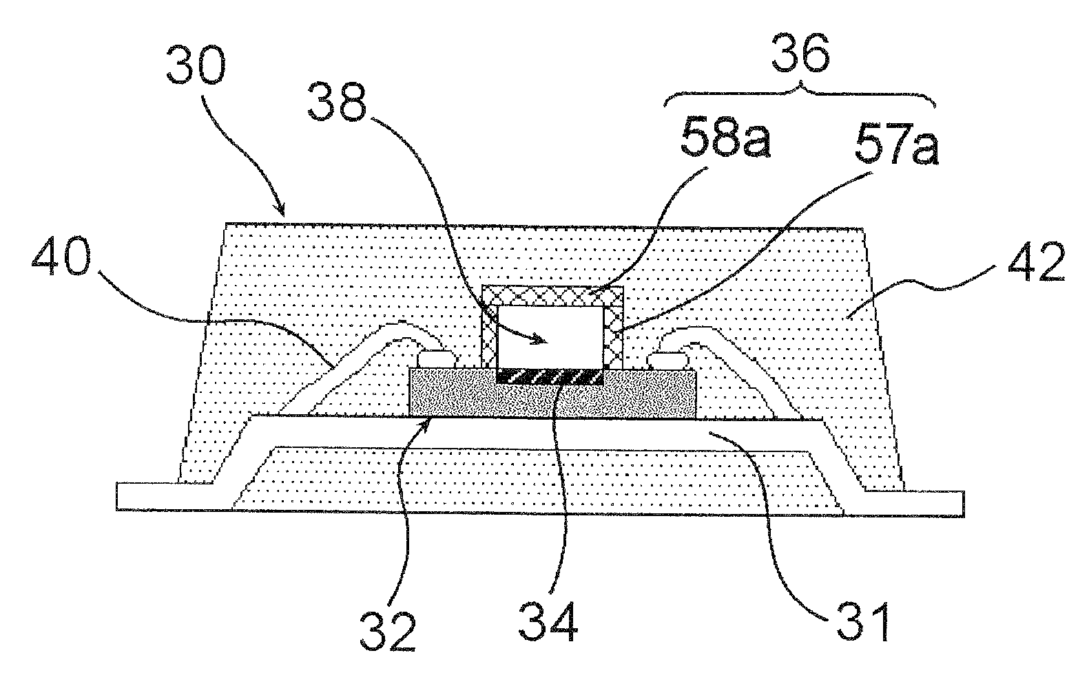
[0028]A semiconductor device of the first embodiment will be explained referring to a sectional view shown in FIG. 1. FIG. 1 shows an exemplary case where a semiconductor device is placed on a lead frame.

[0029]As shown in FIG. 1, a semiconductor device 30 has a semiconductor element 32, a frame component 36 provided over the semiconductor element 32 while forming a cavity 38 therein, and a molding resin layer 42 covering around the frame component 36. Electrode pads of the semiconductor element 32 are electrically connected via wires 40 to a lead frame 31.

[0030]The frame component 36 has a hollow structure composed of a first resin film 57a provided as being risen up around an active region 34 of the semiconductor element 32, and a second resin film 58a tightly closing the space surrounded by the first resin film 57a. As shown in FIG. 3B, given as a partially enlarged view of the frame component 36, the thickness “a” of the first resin film 57a is approximately 5 to 50 μm, and the h...

second embodiment

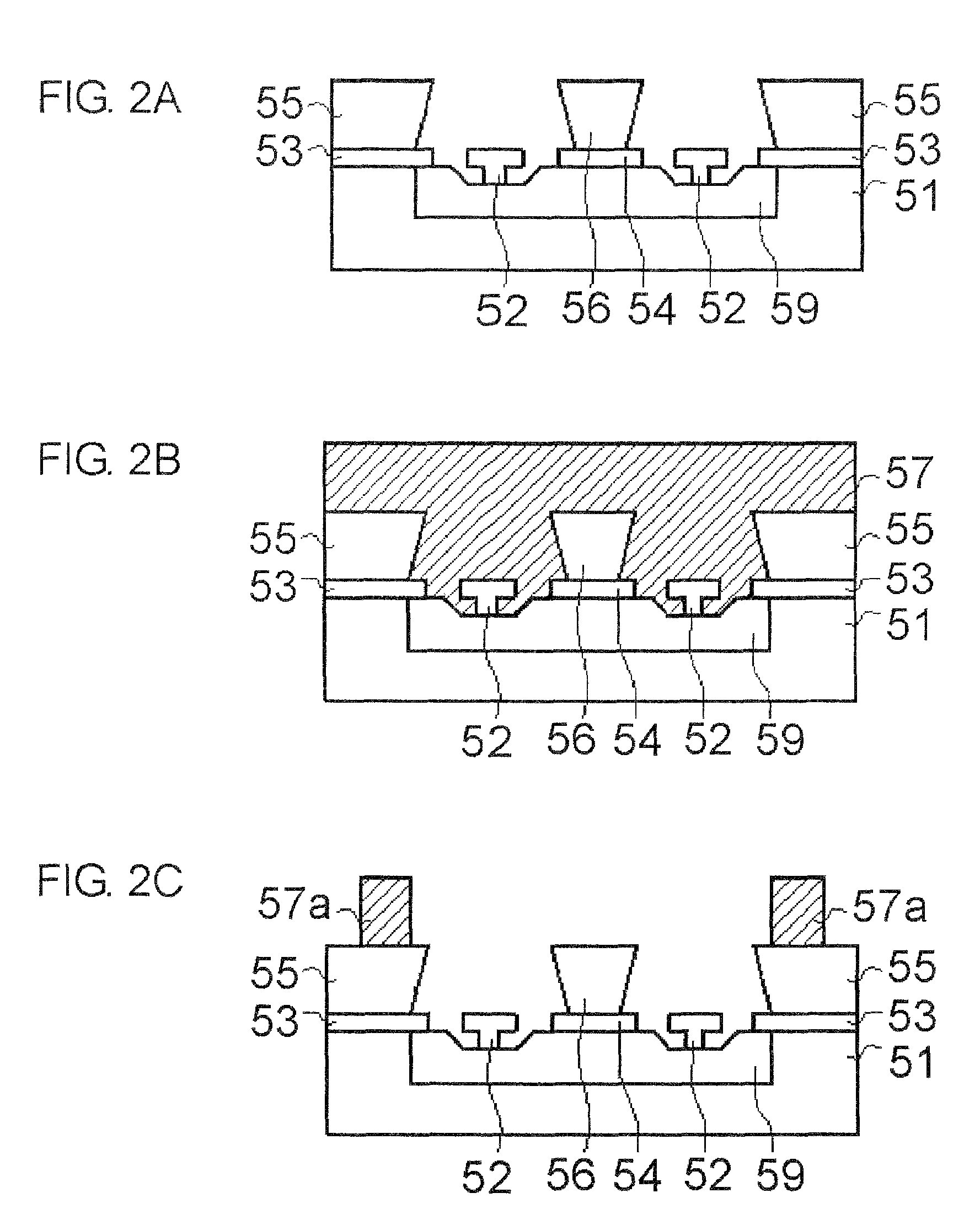
[0067]FIG. 5 shows a semiconductor device of a In this embodiment, the first resin film 57a is left unremoved not only around the gate, but also around the pads. This configuration raises an advantage in that the cavity may be formed in a stable manner, when the photosensitive sheet-like second resin film 58 is bonded.

[0068]FIG. 6 shows a semiconductor device of a third embodiment. In this embodiment, contact area between the first resin film 57a and the second resin film 58a is increased as compared with that in the second embodiment. By virtue of this configuration, adhesiveness between the resins may be made stronger, and thereby yield ratio of the semiconductor device may be improved.

[0069]FIG. 7 shows a semiconductor device of a fourth embodiment. Although this embodiment has a structure different in arrangement of the gates, sources and drain from those in the first to third embodiments, the active region 34 may be covered with the frame component 36 having the cavity 38 ther...


PUM


Abstract

Aiming at providing a semiconductor device advanced in performance of transistors, and improved in reliability, a semiconductor device of the present invention has a semiconductor element, a frame component provided over the semiconductor element, while forming a cavity therein, and a molding resin layer covering around the frame component, wherein the frame component is composed of a plurality of resin films (a first resin film and a second resin film) containing the same resin, and the cavity allows the active region of the semiconductor element to expose therein.

Description

[0001]This application is based on Japanese patent application No. 2007-194127 the content of which is incorporated hereinto by reference.BACKGROUND[0002]1. Technical Field[0003]The present invention relates to a semiconductor device having a semiconductor element packaged therein, and a method of manufacturing the same.[0004]2. Related Art[0005]Minimization of influences of parasitic capacitance may be an effective means for improving performances of transistors. For this purpose, various techniques of reducing the parasitic capacitance, based on covering an active region of a chip using a material having a lower dielectric constant, have been proposed.[0006]For example, a semiconductor device described in Japanese Laid-Open Patent Publication No. H8-070061 has, on an integrated circuit substrate having a semiconductor element mounted thereon, a micro wall of a certain height, risen up on the integrated circuit substrate in the normal direction so as to surround the semiconductor e...

Claims


Application Information

Patent Timeline
Patent Type & Authority Patents(United States)
IPC IPC(8): H01L23/29H01L23/04H01L23/06H01L23/12
CPCH01L21/56H01L23/16H01L23/315H01L23/3135H01L2924/14H01L2924/00014H01L2924/16235H01L2924/181H01L24/48H01L2224/48465H01L2224/48247H01L2924/00H01L2924/00012H01L2224/45099H01L2224/45015H01L2924/207
Inventor KURAMOTO, KAZUNORI
Owner RENESAS ELECTRONICS CORP
Why Eureka
Try Eureka