
Circuit and method for reducing charge injection and clock feed-through in switched capacitor circuits

a switched capacitor and clock feed-through technology, applied in the field of integrated circuits, can solve the problems of limiting the achievable precision of switched capacitor circuits, unwanted charges into nodes, and errors from “charge injection" and achieve the effect of significant reducing both charge injection and clock feed-through

Active Publication Date: 2010-02-16
TEXAS INSTR INC
View PDF19 Cites 12 Cited by
  • Summary
  • Abstract
  • Description
  • Claims
  • Application Information

AI Technical Summary

Benefits of technology

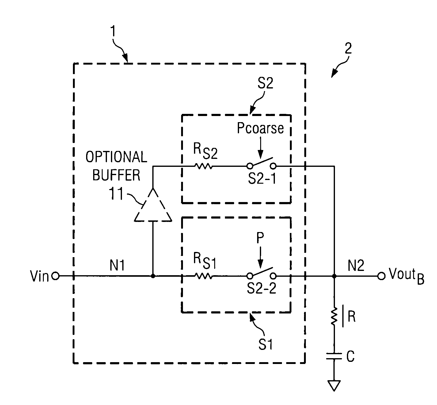
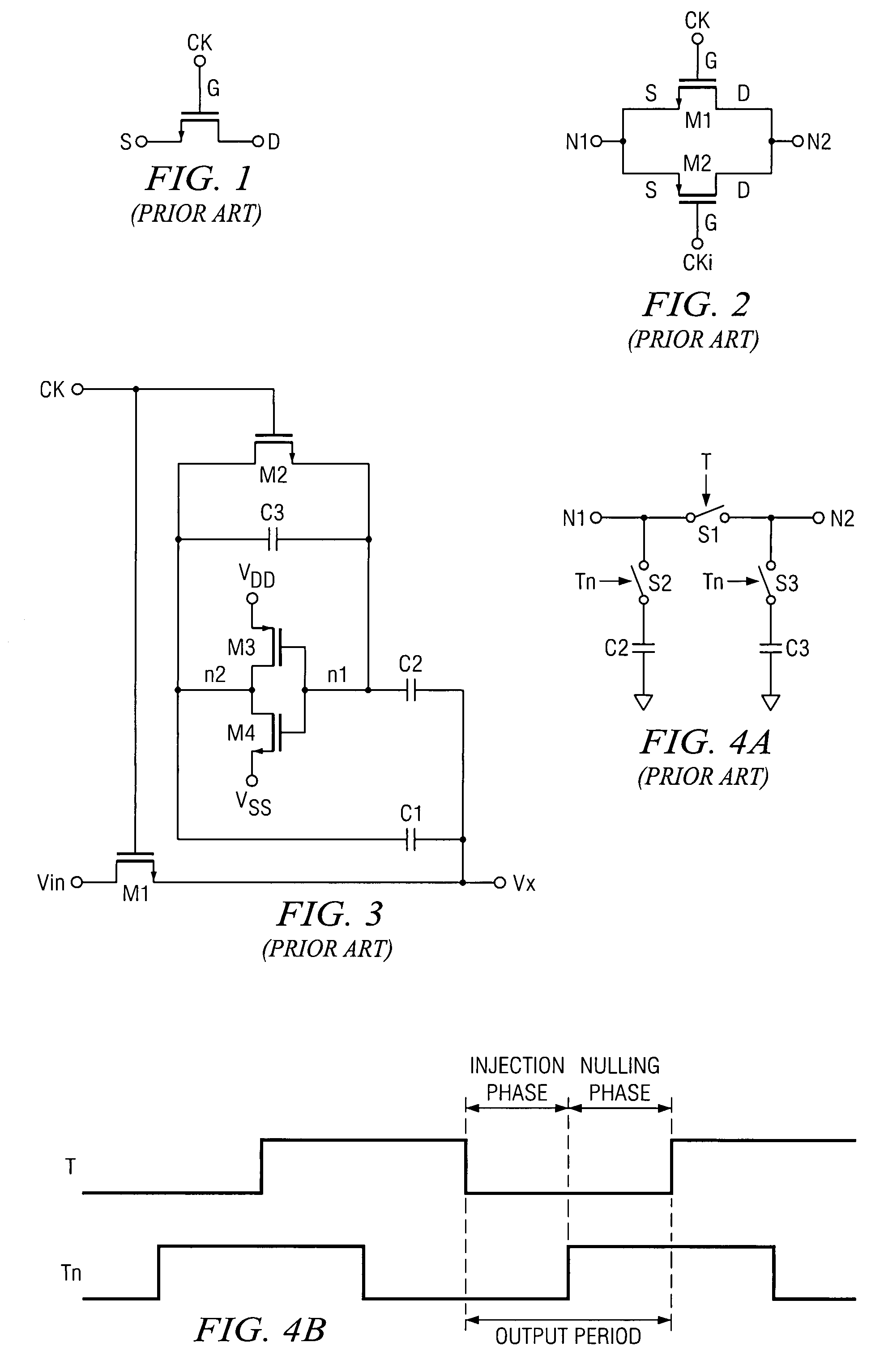
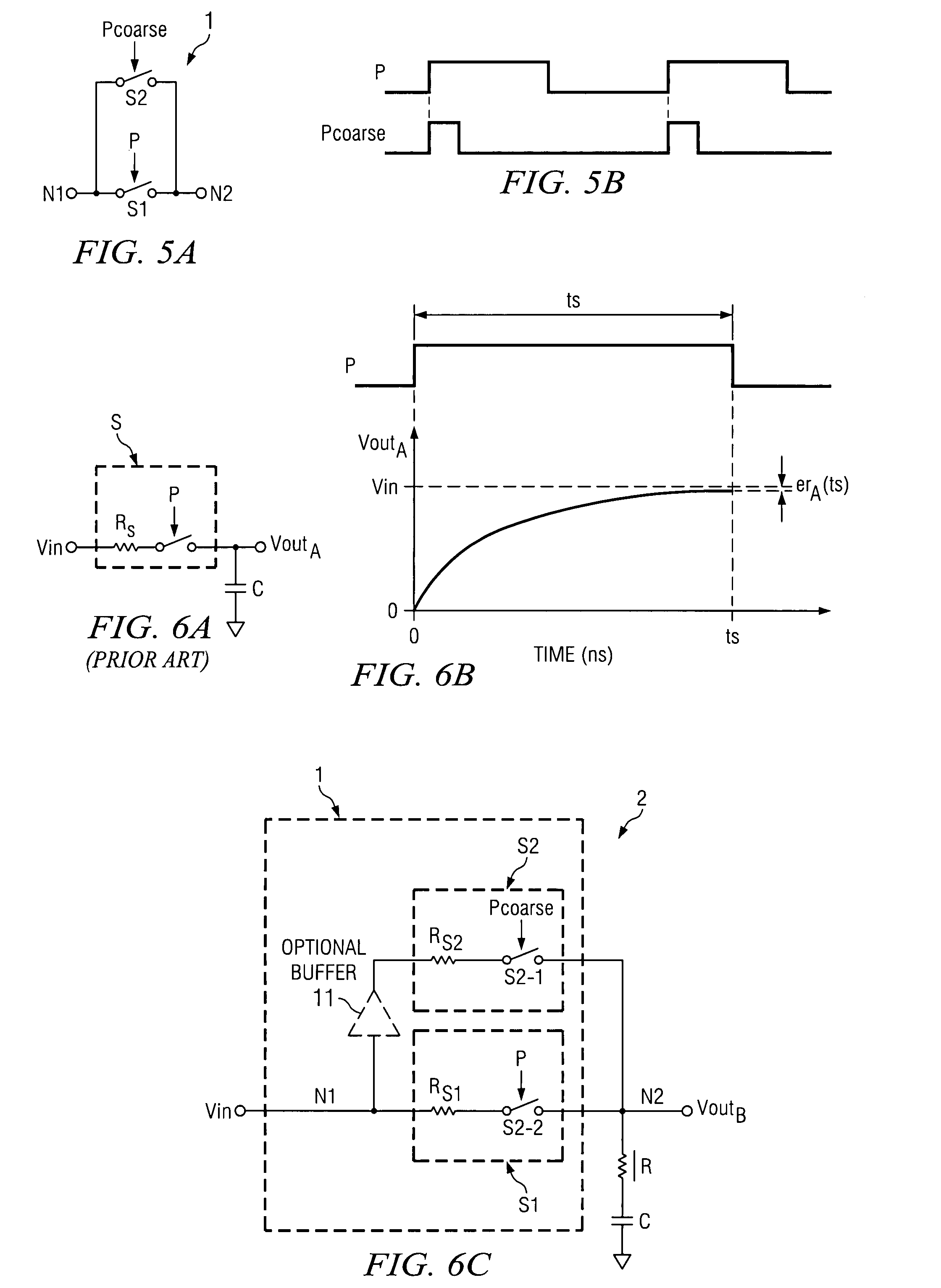
The present invention provides a circuit and technique for reducing charge injection and clock feed-through in switched capacitor integrated circuits. The circuit includes a first and second switching transistor, and a capacitor. The first transistor has a current-carrying electrode coupled to receive a first input signal, a second current-carrying electrode coupled to a second terminal of a sampling capacitor, and a gate coupled to receive a third clock signal. The second transistor has a current-carrying electrode coupled to receive a second input signal. The circuit reduces charge injection and clock feed-through, and requires low power dissipation and small chip layout area.

Problems solved by technology

Two fundamental problems which often limit the achievable precision in switched capacitor circuits are the charge injection and clock feed-through mechanisms associated with the turning off of metal-oxide-semiconductor (MOS) transistor switch elements in the switched capacitor circuits.
Both charge injection and clock feed-through mechanisms introduce unwanted charges into nodes of switched capacitor circuits.
The error due to “clock feed-through” arises specifically from the gate overlap capacitances while the error from “charge injection” arises specifically from the charge that is stored in the channel area of a turned-on MOS transistor.
A first source of the error in a MOS transistor used as a switch in a switched capacitor circuit is the above mentioned channel charge that is “injected” into the source and drain electrodes when the transistor turns off.
A second source of the error in an MOS transistor switch is “clock feed-through” caused by gate-source and gate-drain overlap capacitances of the transistor.
Any mismatch in the three switches and any mismatch in the two capacitors will impair the ability of this circuit to effectively cancel the charge injection and clock feed-through.
Typically the switches are relatively small devices and that means that they cannot be matched very well.
The most notable disadvantages limiting the practicality of known charge injection compensation schemes include (1) relatively large integrated circuit chip layout area required for implementation, (2) increased circuit layout complexity which results in sub-optimal chip layout configurations, (3) the need to rely on matching of compensating switches and / or compensating capacitors for effective charge injection compensation, (4) inability to compensate charge injection in certain circuit topologies and limited ability to compensate charge injection in the other circuit topologies, (5) inability to reduce mismatches in charge injection into differential circuit nodes, and (6) introduction of additional capacitive loading to operational amplifiers used within switched capacitor circuits, resulting in increased power dissipation of the operational amplifiers.
Thus, there is an unmet need for a practical circuit and technique for significantly reducing both charge injection and clock feed-through in switched capacitor integrated circuits.
There also is an unmet need for a practical circuit and technique for significantly reducing both charge injection and clock feed-through in switched capacitor integrated circuits which requires very low power dissipation and which occupies very small amount of chip layout area.

Method used


Image

  • Circuit and method for reducing charge injection and clock feed-through in switched capacitor circuits
  • Circuit and method for reducing charge injection and clock feed-through in switched capacitor circuits
  • Circuit and method for reducing charge injection and clock feed-through in switched capacitor circuits

Examples


embodiment 3

[0072]FIG. 7C shows an embodiment 3 of the invention applied to transistor switch S2 of FIG. 7A to improve both linearity and common-mode rejection of that circuit. As indicated in FIG. 7C, switch S2 is controlled by P1 and switches S1p and S1n are controlled by P1d. In the circuit of FIG. 7C, MOS transistor switch S2coarse, which is controlled by clock signal P1coarse of FIG. 7D, is provided in parallel with MOS transistor switch S2, and the size (i.e., channel width W) of switch S2 is reduced. The size reduction of switch S2 results in proportional reduction of charge injection and clock feed-through and correspondingly results in improved linearity and common-mode rejection of the switched-capacitor circuit 3.

embodiment 4

[0073]FIG. 7E shows an embodiment 4 of the invention applied not only to switch S2 of in FIG. 7A, but also to switches S1p and S1n to further improve both linearity and common-mode rejection of the circuit shown in FIG. 7A. In the switched-capacitor circuit 4 of FIG. 7E the additional switches S1pcoarse and S1ncoarse both controlled by clock signal P1coarse, are provided in parallel with switches S1p and S1n, respectively, and the size W of switches S1p and S1n is reduced. The size reduction of switches S1p and S1n results in proportional reduction of channel charge injection and clock feed-through from those switches and results in further improvement of linearity and common-mode rejection of the switched-capacitor circuit 4.

[0074]FIG. 8A shows another prior art configuration of the differential input-sampling portion of a switched capacitor circuit commonly used, for example, in delta-sigma analog-to-digital converters. FIG. 8B shows the clock signals P1 and P1d. This circuit is s...


PUM


Abstract

A low charge injection, low clock feed-through switch (1) has an input signal (Vin) applied both to the sources of first (S1) and second (2) switching transistors. A first clock signal (P) having pulses of a first duration ts is applied to a gate of the first switching transistor, and a second clock signal (Pcoarse) having pulses of a second duration m×ts substantially less than the first duration is applied to a gate of the second switching transistor. A capacitor (C) is charged toward the input voltage through both the first and second switching transistors during the pulse of the second clock signal. The capacitor is charged further toward the input voltage during a remaining portion of the pulse of the first clock signal.

Description

BACKGROUND OF THE INVENTION[0001]The present invention relates generally to integrated circuits including switched capacitor circuits, and more particularly to circuits and methods for reducing charge injection and clock feed-through in switched capacitor circuits.[0002]An increasing number of modern analog and mixed-signal integrated circuits, such as analog-to-digital converters, digital-to-analog converters, sample-and-hold circuits, and analog filters, use switched capacitor circuits as basic building blocks. The continued demand for improved performance of such analog and mixed-signal circuits has resulted in more stringent requirements for the switched capacitor circuits.[0003]Two fundamental problems which often limit the achievable precision in switched capacitor circuits are the charge injection and clock feed-through mechanisms associated with the turning off of metal-oxide-semiconductor (MOS) transistor switch elements in the switched capacitor circuits. Both charge injec...

Claims


Application Information

Patent Timeline
Patent Type & Authority Patents(United States)
IPC IPC(8): G06F7/64
CPCG11C27/024H03K19/0013H03K19/00361H03K17/16H03K2217/0036
Inventor STULIK, PAUL
Owner TEXAS INSTR INC
Learn More