Advanced multilayer coreless support structures and method for their fabrication

a coreless support and integrated circuit technology, applied in the direction of printed circuit manufacturing, printed circuit aspects, basic electric elements, etc., can solve the problems of increasing the number of input/output contacts, increasing complexity of ics, and increasing the complexity of ics, so as to achieve the effect of large-scale manufacturing

Active Publication Date: 2010-03-23
ZHUHAI ADVANCED CHIP CARRIERS & ELECTRONICS SUBSTRATE SOLUTIONS TECH
View PDF6 Cites 136 Cited by
  • Summary
  • Abstract
  • Description
  • Claims
  • Application Information

AI Technical Summary

Benefits of technology

[0025]It is an aim of the invention to provide a novel manufacturing technique for multilayer interconnect support structures that is economical and is particularly suitable for large scale manufacture.
[0026]It is a further aim to provide a manufacturing technique that attains high yields.
[0027]It is further aim to fabricate arrays of vias between the conductive feature layers without having to ‘drill and plate’, which are time consuming, expensive techniques that are limited to fabricating via shapes having round cross sections.

Problems solved by technology

There is a trend towards ever increasing complexity and ever greater miniaturization in the electronics industry.
As such, ICs are becoming more and more complex, and include ever larger numbers of transistors, and require increasing numbers of input / output contacts.
They are required to operate at ever increasing switching speeds and frequencies, have ever increasing power consumptions and consequently generate ever increasing amounts of heat that requires dissipation.
This is difficult to achieve if the built-up section of the substrate is only formed on one side of the core.
There is a cost to building up layers on both sides of the core however.
It adds more manufacturing process steps, which, in turn, increases fabrication costs.
Since the resulting substrate structure is more complicated, manufacturing yields drop off.
Furthermore, the substrate thickness is increased, resulting in less compact, thicker packages that are less desirable for mobile communication and other applications where miniaturization is required.
This deteriorates the over all performance of the IC.
Firstly, all the conductor layers of the substrate require expensive thin film interconnects.
While conductor layers in the form of thin film interconnects provide better performance due to their improved densities and finer pitches, they are inappropriate to the substrate's power and ground metal planes which are usually low in density and pitch, and building them using expensive thin film technology is cost prohibitive.
Furthermore, these layers usually require a certain metal thickness to reduce electrical resistance and to prevent overheating.
This can become difficult to achieve when using thin film processing techniques.
Furthermore, the Flip Chip bonding process applies a pressure which thin film interconnect structures are ill equipped to withstand.
Such pressures tend to distort and / or stretch the interconnect structure, which in thin films are typically less than 100 microns thick.
This sometimes causes cracking of the thin film dielectric layers and may lead to operating failure of the IC.
Additionally, it will be appreciated that the presence of a metal stiffener adjacent to the IC consumes valuable space on the external surface of the substrate and may limit usage in applications requiring passive components, such as decoupling capacitors, in close proximity to the IC.
Furthermore, the large aperture metal stiffener used may make this technology unsuitable for applications requiring, for example, multi chip substrates, low body-sized substrates, substrates supplied in two dimensional matrix arrays or in strip formats.
Such laminate structures have been found to be susceptible to warping, particularly in consequence of hot pressing or curing processes.
Core-less substrates obtained thereby, typically lack the flatness required for securely and reliably mounting ICs thereupon.
Where such substrates have been built up on one side of a metal carrier base that is subsequently removed prior to IC assembly, or thinned down to provide a stiffener supported substrate, internal unbalanced stresses invariably develop during fabrication.
These stresses may be released on removal of the metal carrier, causing substrate curvature and warping.
This can result in poor yields when assembling the IC thereupon, and may even lead to non flat packages that cannot then be mounted onto the corresponding PCB.
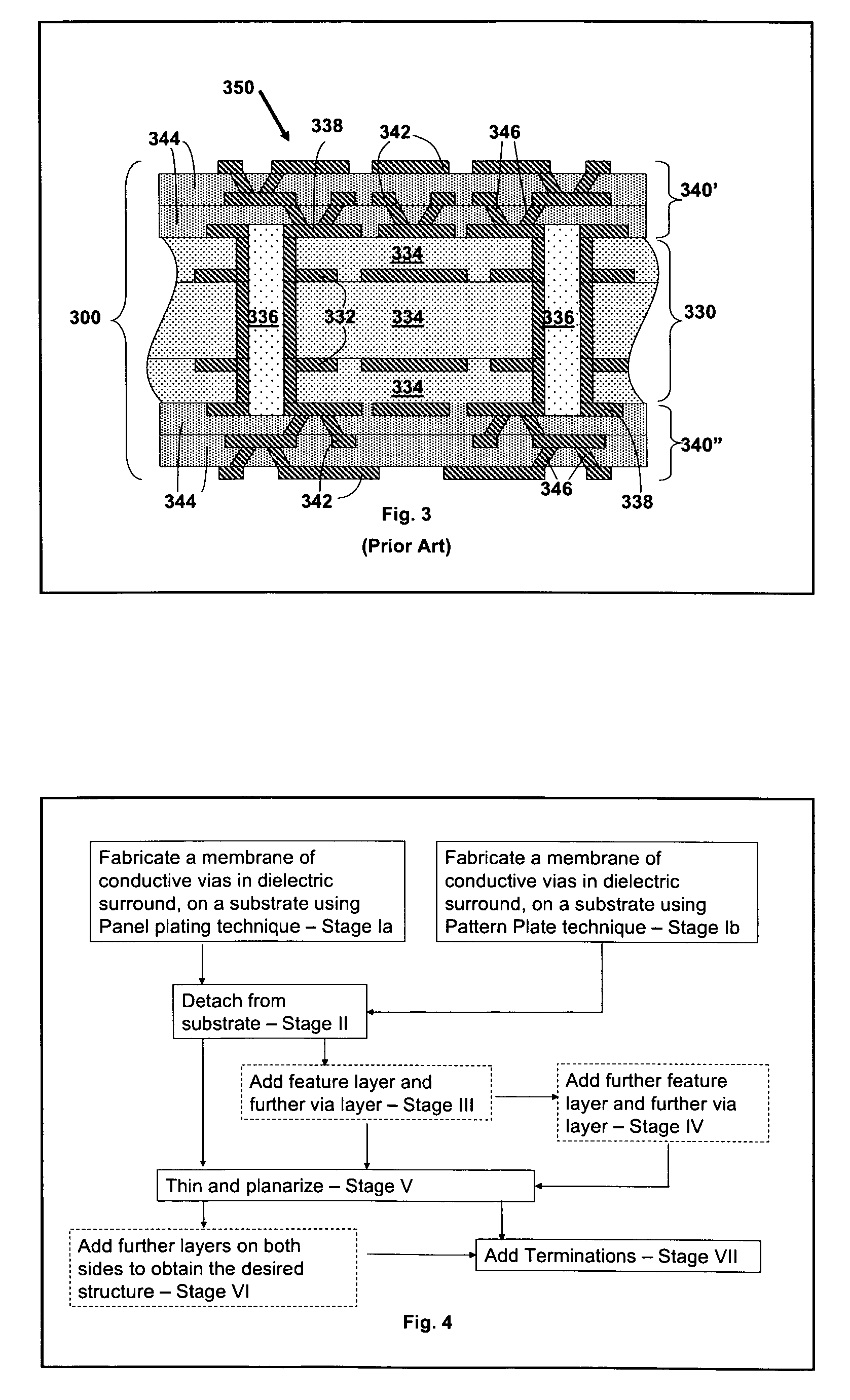
Nevertheless, the technology described in U.S. Pat. No. 6,913,814 to Ho et al. has two major drawbacks: Firstly, in order to construct a structure having a bottom layer with a low pitch BGA thereupon for attachment to a PCB and a high pitch upper IC side, the substrate must be constructed from individual laminae, each having different densities and different dielectric layer thicknesses.
Once again this results in an unbalanced, asymmetrical, structure with an inherent tendency to curving.
Secondly, as is well known to those experienced in the art, connecting the substrate layers with via-to-pad contacts based upon metal contacts achieved through dielectric materials lamination is unreliable for high performance ICs applications, since these have a tendency towards loss of via contact and resultant package failures.
This is especially of concern where high temperature processes are used during IC mounting onto the substrate.
However, because the stack is fabricated from the center outwards, with one half stack being fabricated first, from the center outwards, followed by the second half stack being fabricated on the first half stack, again from the center outwards, it is difficult to ensure that the processing conditions remain the same for the two half stacks, especially for structures with large numbers of layers.
Discrepancies between the two sides typically results in some unbalanced residual stresses in the substrate that may lead to warping, resulting in the substrates that do not reach the strict planarity requirements of advanced IC package constructions, such as Package on Package (PoP), Package in Package (PiP), packages containing stacked ICs, and packages containing several ICs mounted by flip chip processes and others by Wire Bond techniques.
For this and other reasons, the processing method of co-pending IL 171378 to Hurwitz et al., though being a major step forward in the art, nevertheless has limited applicability for very complicated, multilayered structures having a large number of active layers, and attempts to fabricate such structures have, in the past, lead to reduced yields.

Method used


Image

  • Advanced multilayer coreless support structures and method for their fabrication
  • Advanced multilayer coreless support structures and method for their fabrication
  • Advanced multilayer coreless support structures and method for their fabrication

Examples


examples

[0152]With reference to FIG. 12, a schematic cross section through a “2-0-2” symmetrical, coreless support structure having a barrier metal layer 1′ included therein, those results from applying the processing steps of FIG. 10 and FIG. 11 to the variant membrane Ib of FIG. 8. The variant structure of FIG. 12 is similar to that of FIG. 5a, but includes barrier metal layers 1′. It is fabricated by applying the macrostages Ib, II, V, VI and, VII of FIG. 4.

[0153]Referring to FIGS. 13 and 13(I) to 13(xxvii), the process for fabricating the “2-0-2” symmetrical, coreless support structure of FIG. 12 is shown. The steps of constructing the structure of FIG. 12 are first building membrane Ia—steps 13(I) to 13(vi), that are equivalent to the steps of FIG. 9(I) to 9(vi) for fabricating the membrane 8, mutatis mutandis. The structure of 13(vi) is now planarized and thinned, thereby exposing the copper vias—step 13(vii). This step is essentially that of Stage V of FIG. 4. The planarized inner su...


PUM


Abstract

A method of fabricating a free standing membrane including via array in a dielectric for use as a precursor in the construction of superior electronic support structures, includes the steps of fabricating a membrane of conductive vias in a dielectric surround on a sacrificial carrier, and detaching the membrane from the sacrificial carrier to form a free standing laminated array. An electronic substrate based on such a free standing membrane may be formed by thinning and planarizing laminated array, followed by terminating.

Description

FIELD OF THE INVENTION[0001]The present invention is directed to providing support structures for integrated circuits, and to methods for the manufacture thereof.BACKGROUND[0002]There is a trend towards ever increasing complexity and ever greater miniaturization in the electronics industry. Space is at a premium, particularly in mobile equipment such as cellular phones and portable computers.[0003]Integrated Circuits (ICs) are the heart of these electronic systems. As such, ICs are becoming more and more complex, and include ever larger numbers of transistors, and require increasing numbers of input / output contacts. They are required to operate at ever increasing switching speeds and frequencies, have ever increasing power consumptions and consequently generate ever increasing amounts of heat that requires dissipation.[0004]ICs are connected to power supplies, user interfaces and other components via printed circuit boards (PCBs). To facilitate the connection of the IC to the PCB, i...

Claims


Application Information

Patent Timeline
Patent Type & Authority Patents(United States)
IPC IPC(8): H01L21/44
CPCH01L21/4857H01L23/49822H05K3/4682H05K3/4647H01L2924/01047H01L2924/01015H01L2224/32225H01L2224/45147H01L2924/01067H01L2924/01019H01L24/48H05K2203/0733H05K2201/096H05K3/423H05K3/205H01L2924/3011H01L2924/30107H01L2224/16225H01L2224/48227H01L2224/48228H01L2224/48472H01L2224/73204H01L2224/73253H01L2924/0102H01L2924/01046H01L2924/01057H01L2924/01078H01L2924/01079H01L2924/09701H01L2924/15311H01L2924/16152H01L2924/16195H01L2924/19041H01L2924/00H01L2924/00012H01L24/45H01L2224/45015H01L2924/00011H01L2924/00014H01L2924/14H01L2924/181H01L2224/45099H01L2924/01004H01L2924/01033H01L23/48H01L23/58
Inventor HURWITZ, DRORFARKASH, MORDECHAYIGNER, EVASTATNIKOV, BORISMICHAELI, BENNY
Owner ZHUHAI ADVANCED CHIP CARRIERS & ELECTRONICS SUBSTRATE SOLUTIONS TECH
Why Eureka
Try Eureka