Silicon wafer etching method and apparatus, and impurity analysis method
a technology of silicon wafers and etching methods, applied in the direction of electrical equipment, semiconductor/solid-state device testing/measurement, decorative arts, etc., can solve the problems of high degree of sensitivity, inability to analyze metal impurities in samples, and difficulty in uniform in-plane etching, etc., to achieve the effect of little contamination
- Summary
- Abstract
- Description
- Claims
- Application Information
AI Technical Summary
Benefits of technology
Problems solved by technology
Method used
Image
Examples
example 1
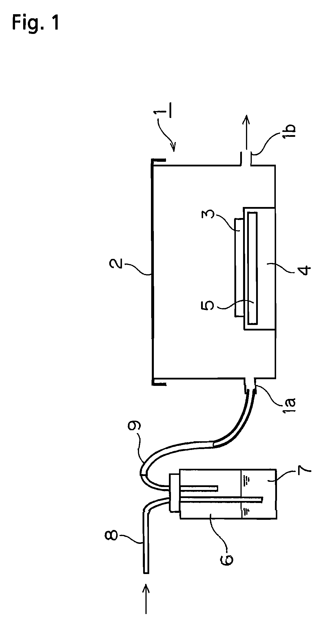
[0056]Using the silicon wafer etching apparatus shown in FIG. 1, the silicon wafer 3, which had been quantitatively contaminated (2 ng) with a standard solution of Fe—Ni—Cu, was placed on the stage 4 in the reaction vessel 1, and the stage 4 and the silicon wafer 3 were cooled to 10° C. with the cooling apparatus 5.
[0057]Meanwhile, the solution 7, which consisted of 100 mL of a 50% hydrofluoric acid solution and 200 mL of a 68% nitric acid solution, was put in the etching chemical container 6, N2 gas was passed through as a carrier gas at a rate of 1 L / min, and exhaust was performed at 100 hPa.
[0058]Various holding times were tested in this etching gas introduction and exhaust state. After this, just N2 gas was allowed into the reaction vessel 1 for 15 minutes to replace the system with N2 gas, after which the lid 2 was opened and the silicon wafer 3 was taken out, and the amount of etching was measured.
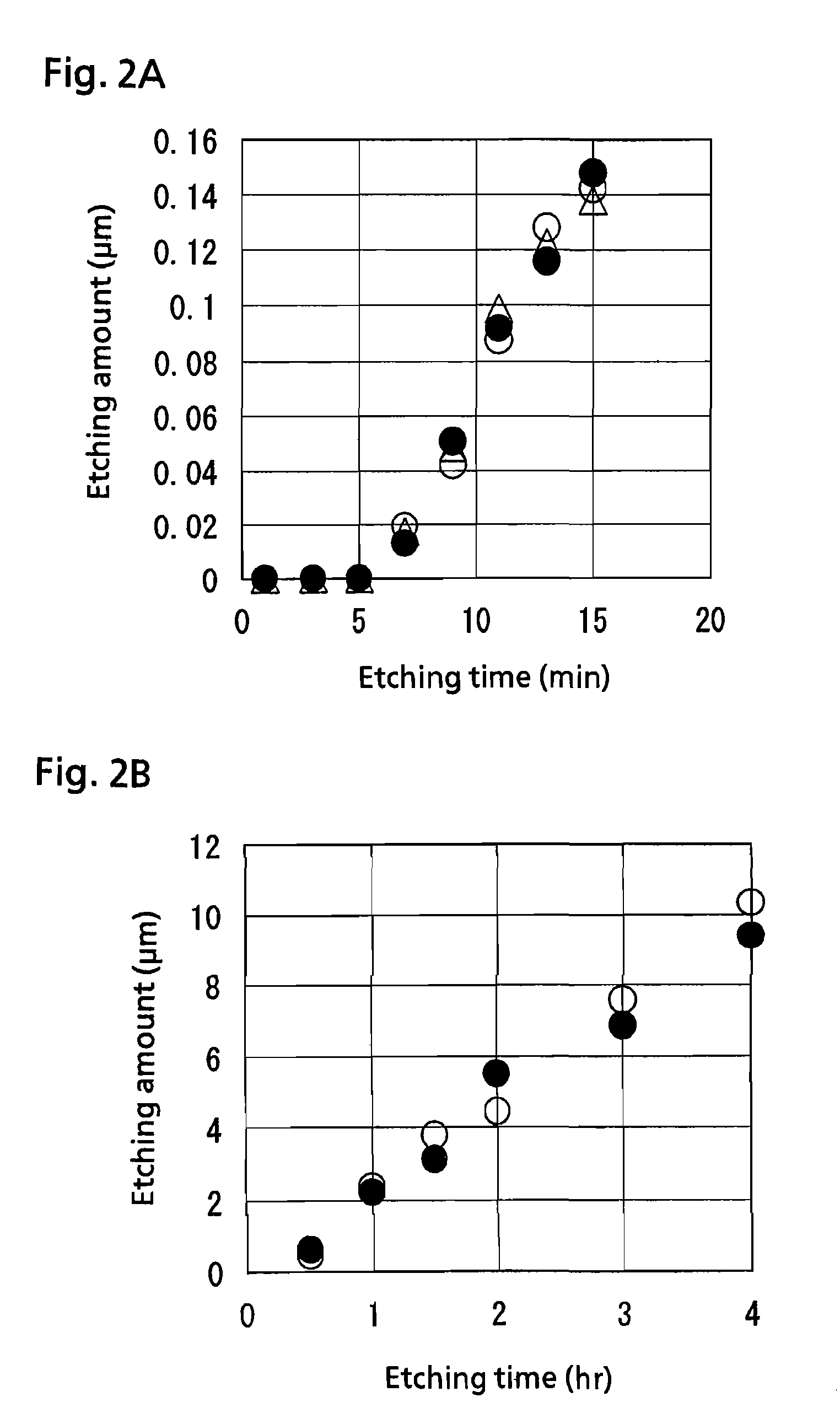
[0059]FIGS. 2A and 2B show the relation between the amount of etching and the et...
example 2
[0061]The various silicon wafers before and after the etching performed for various holding times in Example 1 were measured for thickness (ADE measurement), and the in-plane distribution of the amount of etching of the wafer during etching was examined.
[0062]FIG. 4 shows the wafer in-plane etching amount distribution, and FIG. 5 shows the etching amount and the in-plane uniformity (CV %) of the etching amount. As a result, it can be seen that the wafer in-plane etching uniformity was good (a CV % of no more than 10%) for all wafers.
[0063]The surface roughness after etching was also examined by AFM measurement. FIG. 6 shows an image produced by AFM measurement of a wafer that has been etched by 0.2 μm. FIG. 7 is a graph of the wafer etching amount and the surface roughness. As a result, it can be seen that the surface roughness was good, since the Rms is no more than 10% of the etching amount at all etching amounts.
[0064]In Example 1, etching (2 μm) was performed by holding for 1 ho...
PUM
| Property | Measurement | Unit |
|---|---|---|
| temperature | aaaaa | aaaaa |
| depth | aaaaa | aaaaa |
| surface roughness | aaaaa | aaaaa |
Abstract
Description
Claims
Application Information


