Silicon wafer etching method and apparatus, and impurity analysis method

Active Publication Date: 2008-02-28
SUMITOMO MITSUBISHI SILICON CORP
View PDF12 Cites 4 Cited by
  • Summary
  • Abstract
  • Description
  • Claims
  • Application Information

AI Technical Summary

Benefits of technology

[0016] It is an object of the present invention to solve the above-mentioned problems encountered in etching by an indirect dissolution method, and to provide a method for etching a silicon wafer. With this method, the amount of in-plane etching can be uniform, and there is little contamination during the concentration of the recovered solution. Therefore, a high-precision and high-sensitivity analysis can be possible. It is a further object of the present invention to provide an apparatus used in the above-mentioned etching method, as well as an impurity analysis method that utilizes the above-mentioned etching method.
[0018] Also, the inventors perfected the present invention by adjusting the hydrofluoric acid and nitric acid in an etching solution—which is bubbled with a carrier gas without being heated—to a specific molar ratio, and regulating the amount of gas by the above-mentioned means as the gas is introduced, and cooling all or a specific portion of the silicon wafer to between 0 and 20° C. to condense the gas on its surface. As a result, the required portion of the wafer can be etched, with a uniform amount of the required in-plane etching, so the wafer surface will have good smoothness after etching, the amount of recovery liquid can be reduced, and the amount of admixed silicon during impurity analysis, the concentration time, and so forth can be decreased.

Problems solved by technology

However, with direct dissolution, the liquid is dropped over the entire surface of the silicon wafer, so a large amount of chemical must be used, metal impurities present in the chemical itself pose a substantial background to the analysis values, and the metal impurities in the sample cannot be analyzed to a high degree of sensitivity.
With this method, very little liquid is dropped ((just several hundred microliters), so uniform in-plane etching is difficult, and there is considerable variance in the amount of etching from one silicon wafer to the next.
Some of the problems with this method are that it is difficult to control the amount of gas generated, which affects the amount of etching of the silicon wafer and prevents uniform etching of the surface, and etching unevenness makes it difficult to recover the subsequent decomposition residue with a chemical.
A problem with this method, however, is that adequate etching performance cannot be achieved (approximately 0.1 μm / hr) because the nitric acid and hydrofluoric acid gases are supplied separately.
A problem with this method, however, is that the nitric acid and hydrofluoric acid gas is generated by heating the vessel of the nitric acid and hydrofluoric acid, and it is difficult to control the amount of gas generated, which affects how much the silicon wafer is etched and prevents the surface from being etched uniformly.
In addition, there is a method in which the condensed liquid is analyzed directly with an atomic absorption spectrometer, but the condensed liquid contains a large HF and silicon component, which poses a substantial background during analysis, the peak shape for the sample becomes abnormal, etc., making quantitative analysis difficult.
However, since this concentration method involves the use of a large quantity of chemical, there is the danger that the metal impurities contained in the chemical will contaminate the concentrate, and there is also the possibility that long-term concentration will result in contamination from the atmosphere.

Method used


Image

  • Silicon wafer etching method and apparatus, and impurity analysis method
  • Silicon wafer etching method and apparatus, and impurity analysis method
  • Silicon wafer etching method and apparatus, and impurity analysis method

Examples


example 1

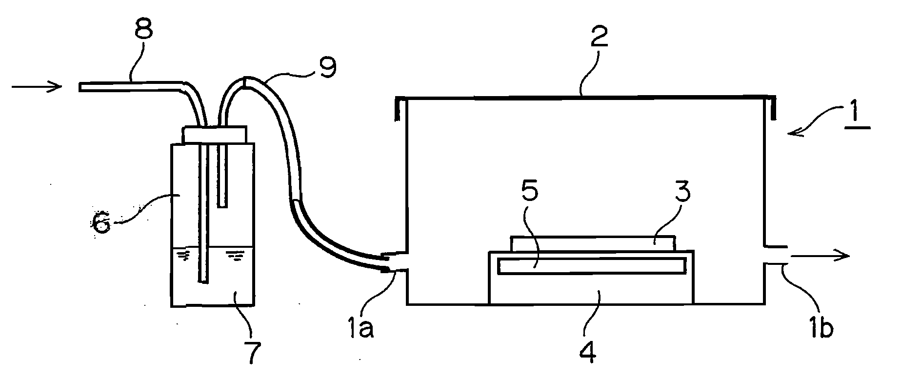
[0056] Using the silicon wafer etching apparatus shown in FIG. 1, the silicon wafer 3, which had been quantitatively contaminated (2 ng) with a standard solution of Fe—Ni—Cu, was placed on the stage 4 in the reaction vessel 1, and the stage 4 and the silicon wafer 3 were cooled to 10° C. with the cooling apparatus 5.

[0057] Meanwhile, the solution 7, which consisted of 100 mL of a 50% hydrofluoric acid solution and 200 mL of a 68% nitric acid solution, was put in the etching chemical container 6, N2 gas was passed through as a carrier gas at a rate of 1 L / min, and exhaust was performed at 100 hPa.

[0058] Various holding times were tested in this etching gas introduction and exhaust state. After this, just N2 gas was allowed into the reaction vessel 1 for 15 minutes to replace the system with N2 gas, after which the lid 2 was opened and the silicon wafer 3 was taken out, and the amount of etching was measured.

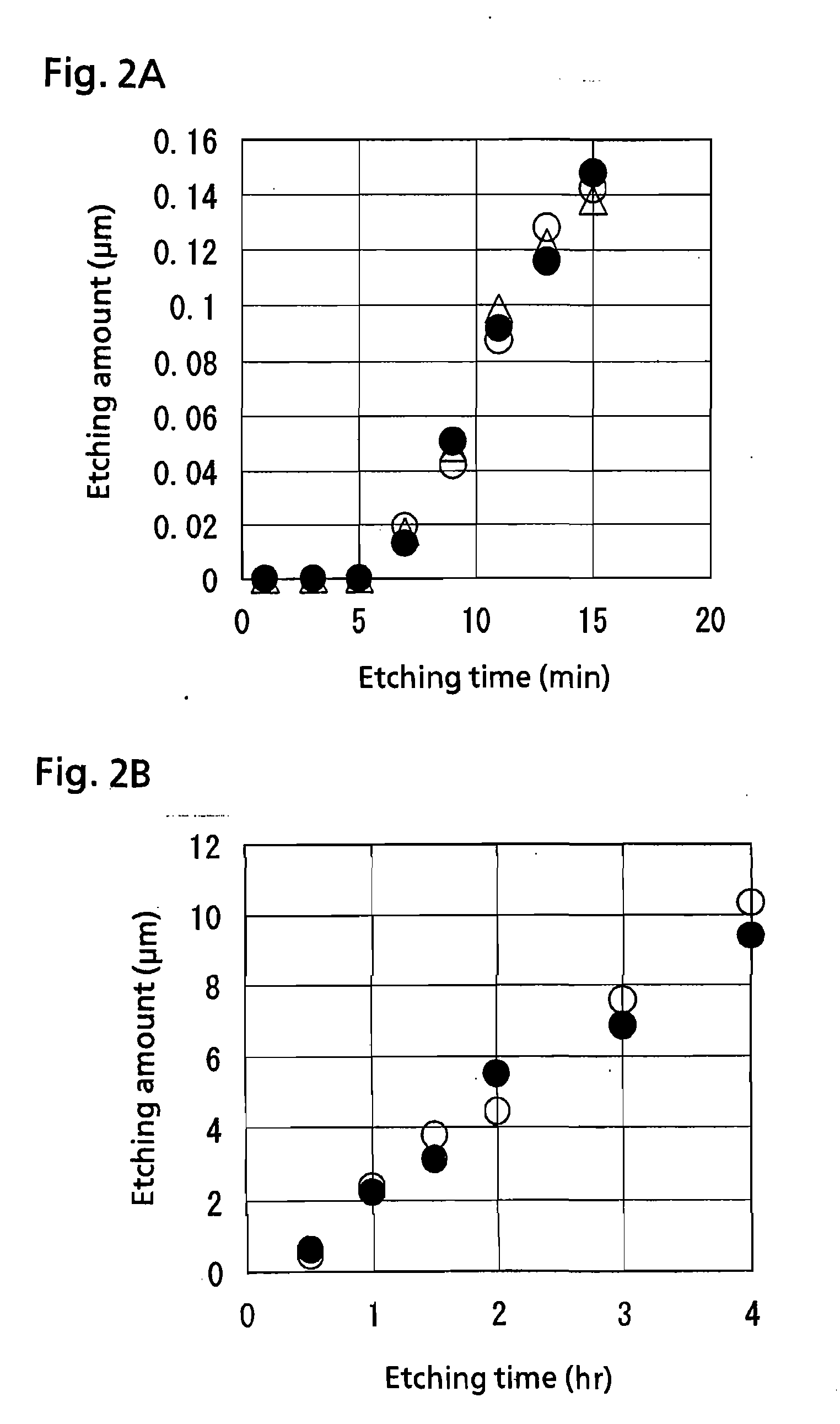
[0059]FIGS. 2A and 2B show the relation between the amount of etching and ...

example 2

[0061] The various silicon wafers before and after the etching performed for various holding times in Example 1 were measured for thickness (ADE measurement), and the in-plane distribution of the amount of etching of the wafer during etching was examined.

[0062]FIG. 4 shows the wafer in-plane etching amount distribution, and FIG. 5 shows the etching amount and the in-plane uniformity (CV %) of the etching amount. As a result, it can be seen that the wafer in-plane etching uniformity was good (a CV % of no more than 10%) for all wafers.

[0063] The surface roughness after etching was also examined by AFM measurement. FIG. 6 shows an image produced by AFM measurement of a wafer that has been etched by 0.2 μm. FIG. 7 is a graph of the wafer etching amount and the surface roughness. As a result, it can be seen that the surface roughness was good, since the Rms is no more than 10% of the etching amount at all etching amounts.

[0064] In Example 1, etching (2 μm) was performed by holding fo...


PUM

PropertyMeasurementUnit
Temperatureaaaaaaaaaa
Lengthaaaaaaaaaa
Volumeaaaaaaaaaa

Abstract

A wafer etching and impurity analysis method is presented in which a wafer is held in a vessel having gas introduction and exhaust ports, a solution including a mixture of hydrofluoric acid and nitric acid alone or together with sulfuric acid is bubbled with a carrier gas without being heated, which generates a gas containing vaporized hydrofluoric acid and nitric acid, and the inside of the vessel is purged so that the amount of gas supplied is kept constant at all times. All or a specific portion of the wafer is cooled to a specific temperature. Consequently, the gas is condensed on the surface of the wafer, which allows the required portion of the wafer to be etched. The method reduces the amount of liquid needed for residue recovery, the amount of admixed silicon during impurity analysis, and the concentration time.

Description

CROSS-REFERENCES TO RELATED APPLICATIONS [0001] This application is a continuation-in-part of U.S. patent application Ser. No. 10 / 489,763, filed Mar. 11, 2004, which is a U.S. national phase application under 35 U.S.C. §371 of International Patent Application No. PCT / JP02 / 10904 filed Oct. 21, 2002, and claims the benefit of Japanese Patent Application No. 2001-325863 filed Oct. 24, 2001. The International Application was published in Japanese on May 1, 2003 as WO 03 / 036706 A1 under PCT Article 21(2). All of the aforementioned documents are incorporated herein by reference.FIELD OF THE INVENTION [0002] This invention relates to an etching method with which a recovered solution of decomposition residue after a silicon wafer surface has been etched is analyzed and the metal impurities contained in the silicon wafer are quantitatively analyzed. The invention further relates to an etching method and apparatus and an impurity analysis method. The method produces an amount of in-plane etch...

Claims


Application Information

Patent Timeline
IPC IPC(8): C23F1/00B44C1/22H01L21/302H01L21/66H01L21/306
CPCH01L21/30604H01L21/02019
Inventor HIRANO, KATSUYAHORIE
Owner SUMITOMO MITSUBISHI SILICON CORP
Why Eureka
Try Eureka