Method of eliminating small bin defects in high throughput TEOS films

a technology of teos film and bin defect, which is applied in the direction of coating, chemical vapor deposition coating, metallic material coating process, etc., can solve the problems of reducing yield, reducing yield, and causing yield problems, so as to reduce the number of particles, eliminate or minimize small bin defects, and achieve high throughput pecvd

Active Publication Date: 2010-04-27
NOVELLUS SYSTEMS
View PDF8 Cites 45 Cited by
  • Summary
  • Abstract
  • Description
  • Claims
  • Application Information

AI Technical Summary

Benefits of technology

[0008]The present invention meets these needs by providing a high throughput PECVD process for depositing TEOS films in a multi-station sequential deposition chamber. In many embodiments, the methods significantly reduce the number of particles in the TEOS films, thereby eliminating or minimizing small bin defects. An example method involves dedicating a first station for temperature soak while flowing purge gas. Stopping the flow of reactant gas and flowing the purge gas for station 1 may eliminate TEOS condensation on a cold wafer surface and significantly reduce the number of defects in the film, particularly for short temperature soaks.

Problems solved by technology

Because SiN has poor conformal properties, when deposited on a wafer it highlights defects that ordinarily may not have been visible by some optical detection methods.
As device size shrinks to 65 nanometers and below, small bin size defects can greatly reduce yield.
Even more yield problems can arise as the number of integration layers increase; the upper layers magnify small bin defects from lower layers to become large bin defects.
However, the advantage of high throughput would be lost.

Method used


Image

  • Method of eliminating small bin defects in high throughput TEOS films
  • Method of eliminating small bin defects in high throughput TEOS films
  • Method of eliminating small bin defects in high throughput TEOS films

Examples


Embodiment Construction

Introduction

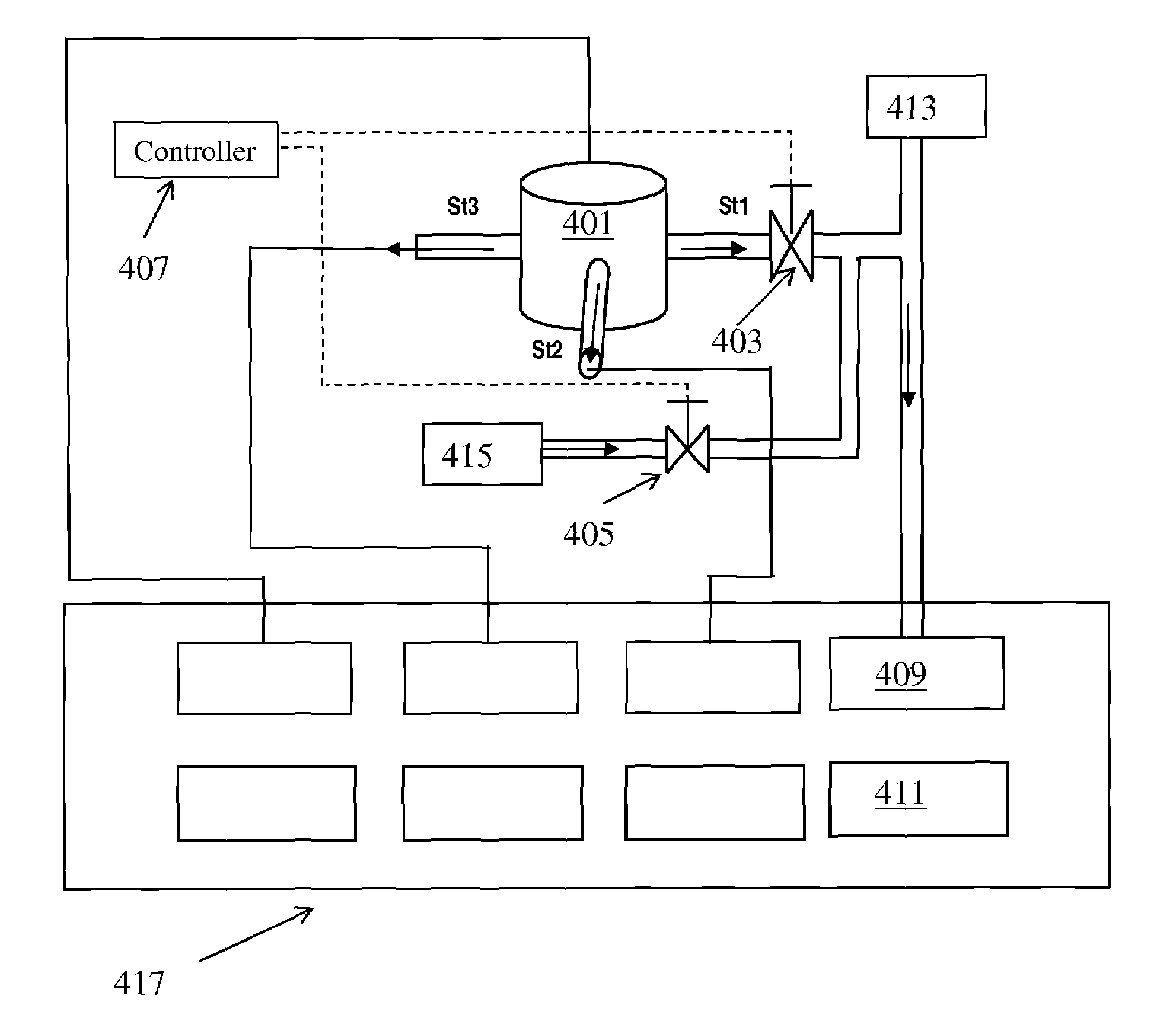
[0025]In the following detailed description of the present invention, numerous specific embodiments are set forth in order to provide a thorough understanding of the invention. However, as will be apparent to those skilled in the art, the present invention may be practiced without these specific details or by using alternate elements or processes. In other instances well-known processes, procedures and components have not been described in detail so as not to unnecessarily obscure aspects of the present invention.

[0026]In this application, the terms “substrate” and “wafer” will be used interchangeably.

[0027]The following detailed description assumes the invention is implemented on a semiconductor wafer. However, the invention is not so limited. The work piece may be of various shapes, sizes, and materials. In addition to semiconductor wafers, other work pieces that may take advantage of this invention include various articles such as display front planes printed circuit ...


PUM

PropertyMeasurementUnit
sizeaaaaaaaaaa
temperatureaaaaaaaaaa

Abstract

This invention provides a high throughput PECVD process for depositing TEOS films in a multi-station sequential deposition chamber. The methods significantly reduce the number of particles in the TEOS films, thereby eliminating or minimizing small bin defects. The methods of the invention involve dedicating a first station for temperature soak while flowing purge gas. Stopping the flow of reactant gas and flowing the purge gas for station 1 eliminates TEOS condensation on a cold wafer surface and significantly reduces the number of defects in the film, particularly for short temperature soaks.

Description

FIELD OF THE INVENTION[0001]The present invention pertains to methods for depositing dielectric film on a substrate. More specifically, the invention pertains to high throughput PECVD TEOS processes. The invention is effective at eliminating small bin defects in thin PECVD TEOS films.BACKGROUND[0002]TEOS (tetra-ethyl-ortho-silicate) is a silicon-containing compound that is a liquid at room temperature. TEOS is used in many applications to deposit dielectric film on a substrate. TEOS is used in applications where conformality is required as silicon dioxide (or “TEOS oxide”) films deposited by TEOS chemical vapor deposition processes have good conformality. TEOS oxide is often deposited by a plasma enhanced deposition chemical vapor deposition (PECVD) process. TEOS-based PECVD processes typically involve exposing a substrate to a process gas including TEOS and an oxidant such as oxygen or ozone. Liquid TEOS is first vaporized in a preheater to about 150 degrees Celsius. TEOS vapor flo...

Claims


Application Information

Patent Timeline
Patent Type & Authority Patents(United States)
IPC IPC(8): H01L21/461
CPCC23C16/402C23C16/50H01L21/31612H01L21/02274H01L21/0228H01L21/02164
Inventor HENRI, JONTANG, XINGYUANTIAN, JASONGERBER, KEVINDHAS, ARUL N.
Owner NOVELLUS SYSTEMS
Why Eureka
Try Eureka