
Microstructure synthesis by flow lithography and polymerization

a microstructure and lithography technology, applied in the field of polymer materials, can solve the problems of limiting the composition and/or the through-put of such processes is typically limited, and the photolithography techniques generally limit the compatibility of the microstructure material, etc., to achieve the effect of superior control of the geometry of the microstructure, shape, composition and anisotropy

Active Publication Date: 2010-05-04
MASSACHUSETTS INST OF TECH
View PDF12 Cites 128 Cited by
  • Summary
  • Abstract
  • Description
  • Claims
  • Application Information

AI Technical Summary

Benefits of technology

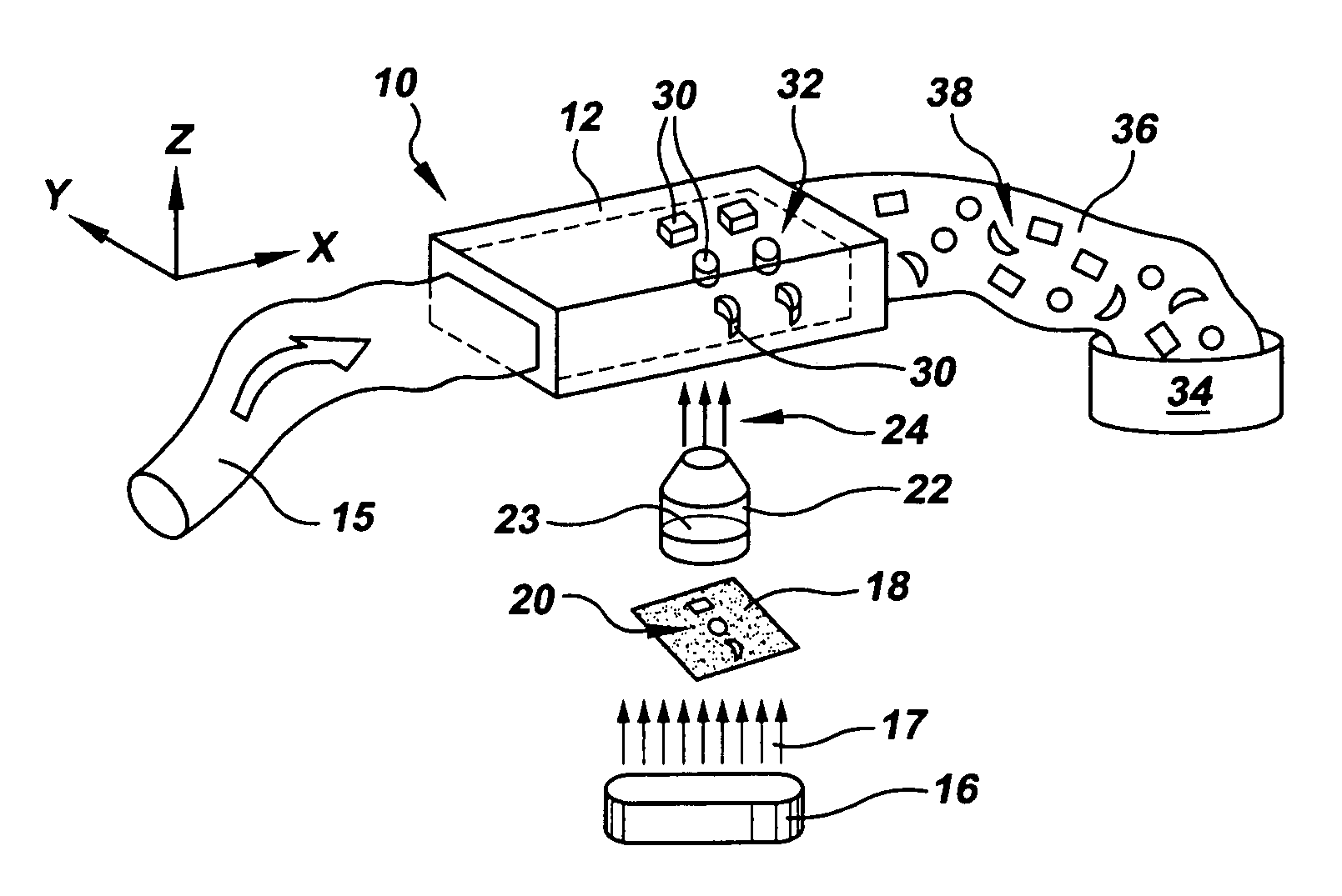
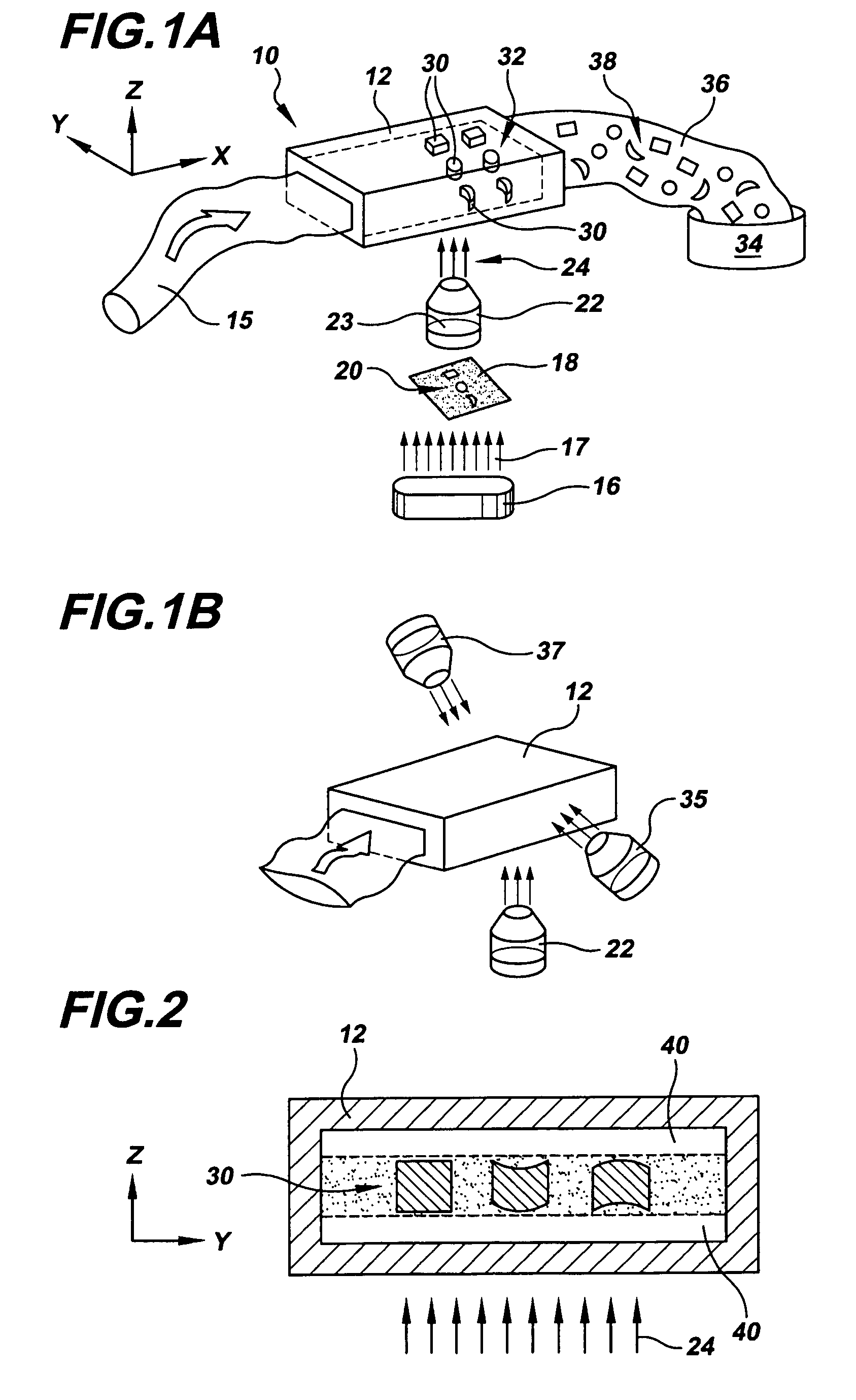
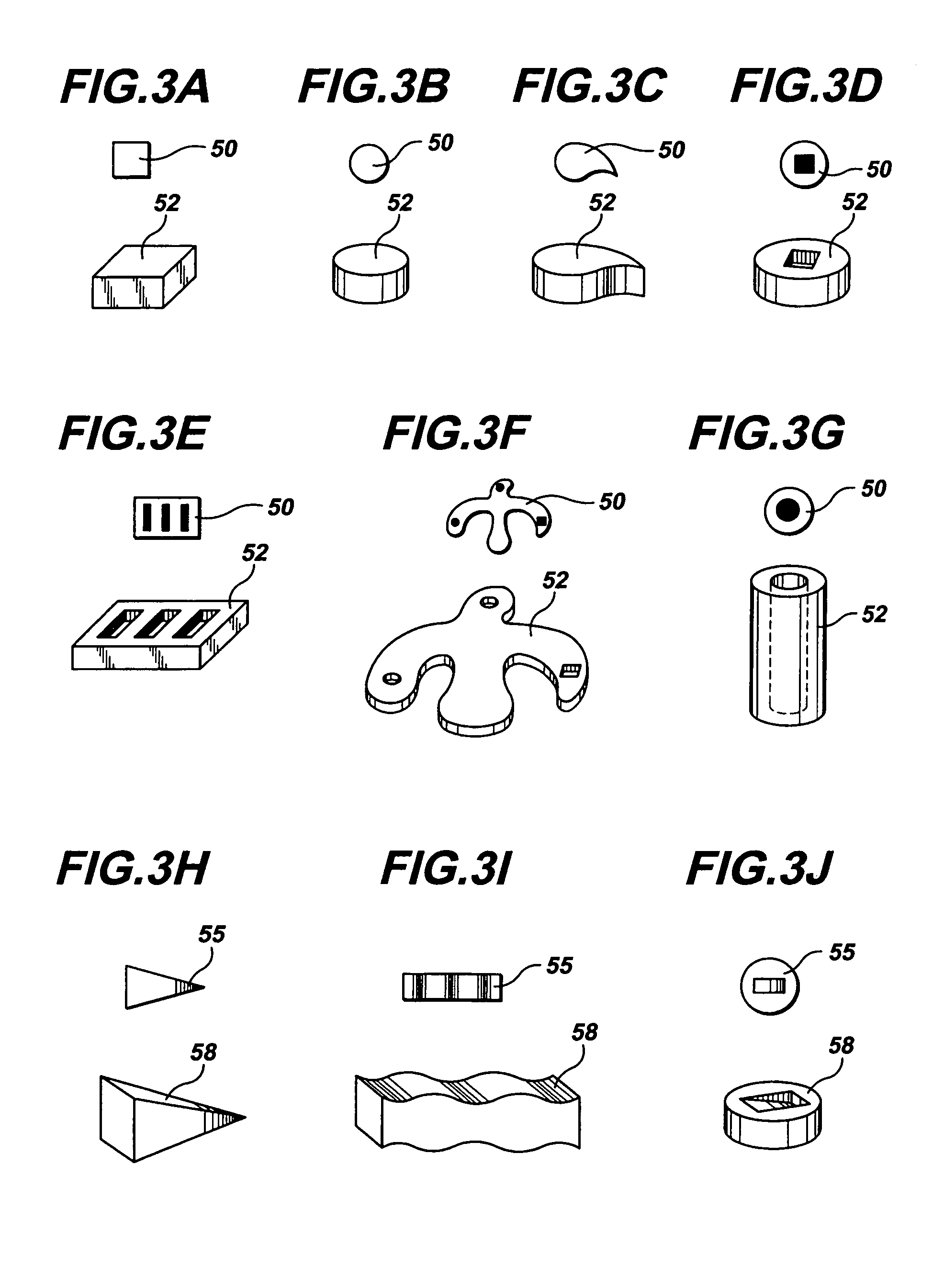
The invention provides a new method for making polymeric microstructures with complex shapes and chemistries. This method uses a laser to create microstructures in a continuous process. The laser creates a shape in the material as it flows through a channel, and the shape is preserved when the material solidifies. This method allows for better control over the microstructure's shape, composition, and anisotropy. It can also produce non-spheroidal microstructures with multiple material regions and planar microstructures with multiple material regions. Overall, this invention provides a faster and more precise way to make polymeric microstructures.

Problems solved by technology

Although these techniques have provided significant advances in microstructure synthesis, it is found in general that each limits microstructure composition and / or geometry.
For example, photolithographic techniques generally limit the microstructure material to that which is compatible with a photolithographic process, e.g., requiring a photoresist as the structural material.
In addition to these limitations in polymeric microstructure composition and geometry, conventional polymeric microstructure synthesis generally requires isotropic structural arrangements of materials.
Further, the through-put of such processes is typically limited by a requirement for making one structure at a time or a limited photo-mask-defined field of structures at a time.
These limitations in polymeric microstructure synthesis through-put, microstructure geometry, morphology, and functionality have restricted the ability to address the growing number of critical applications for which polymeric microstructures could be well suited.

Method used


Image

  • Microstructure synthesis by flow lithography and polymerization
  • Microstructure synthesis by flow lithography and polymerization
  • Microstructure synthesis by flow lithography and polymerization

Examples


example i

[0104]A number of microfluidic devices were fabricated by first patterning a silicon substrate with photoresist, SU-8, from Microchem, Newton, Mass., to define a mold structure corresponding to a rectangular microfluidic device cross section as in FIG. 6A. PDMS provided as Sylgard®184 silicon elastomer, from Dow Corning, Midland, Mich., was poured into the resulting positive-relief channels of the silicon substrate to mold an upper PDMS device structure 100 as in FIG. 6A. Rectangular microfluidic devices of 1 cm in length and three different channel widths were defined by the patterning, namely, 20 μm-wide, 600 μm-wide, and 1000 μm-wide, and three different rectangular microfluidic channel heights were defined by the patterning, namely, 10 μm in height, 20 μm in height, and 40 μm in height A layer of PDMS was spin-coated on glass slides to form bottom surfaces for the microfluidic devices as in FIG. 6A. The molded upper PDMS device structures were mated with PDMS-coated glass slides...

example ii

[0115]Square polymeric microstructures were synthesized in the manner of Example I with square mask features ranging in edge length from 10 μm to 500 μm. The microstructure synthesis was duplicated for a 20× objective and a 40× objective. The three microfluidic devices described in Example I were employed, having channel heights of 10 μm, 20 μm, and 40 μm. The PEG-DA and DAROCUR® 1173 photoinitiator monomer stream of Example I was employed in the microfluidic devices, with the steam flow stopped during the lithography-polymerization step, in the stop flow process described above. The resulting microstructures were collected and analyzed as in Example I.

[0116]The microstructure analysis was conducted to determine the smallest mask feature that could be polymerized at a given exposure time in the channels of varying height. FIG. 11A is a plot of the smallest mask feature that could be polymerized, as a function of exposure time, for the 20× objective; FIG. 11B is a plot of the smalles...

example iii

[0117]One of the microfluidic devices of Example I having a cross section channel height of 38 μm (intended as 40 μm) was adapted by replacing the PDMS-coated glass slide with an uncoated glass slide, and polymeric microstructure synthesis was carried out with the monomer as in Example I. It was found that the synthesized microstructures stuck to the glass plate. This result is recognized to be due to the absence of the oxygen inhibition effect enabled by the PDMS coating in Example I, thereby allowing the synthesized microstructures to polymerize all the way to the glass surface.

[0118]Polymeric microstructures were synthesized in the manner of Example I with a PDMS-coated glass slide device and with an uncoated glass slide device, both having a cross-sectional channel height of 38 μm. An exposure time, texp, of 0.1 s, a 360 μm square mask shape, and a 20× objective were employed with each of the two devices.

[0119]Microstructures synthesized with the two microfluidic devices were co...


PUM

PropertyMeasurementUnit
sizeaaaaaaaaaa
thicknessaaaaaaaaaa
thicknessaaaaaaaaaa

Abstract

In a method for synthesizing polymeric microstructures, a monomer stream is flowed, at a selected flow rate, through a fluidic channel. At least one shaped pulse of illumination is projected to the monomer stream, defining in the monomer stream a shape of at least one microstructure corresponding to the illumination pulse shape while polymerizing that microstructure shape in the monomer stream by the illumination pulse.

Description

CROSS-REFERENCE TO RELATED APPLICATIONS[0001]This application claims the benefit of U.S. Provisional Application No. 60 / 730,052, filed Oct. 25, 2005, the entirety of which is hereby incorporated by reference.STATEMENT REGARDING FEDERALLY SPONSORED RESEARCH[0002]This invention was made with Government support under Contract No. CTS-0304128 awarded by NSF. The Government has certain rights in the invention.BACKGROUND OF INVENTION[0003]This invention relates generally to polymer materials, and more particularly relates to techniques for synthesizing polymeric microstructures.[0004]Polymeric microstructures are important for a wide range of applications, including MEMS, biomaterials, drug delivery, self-assembly, and other applications. The ability to controllably synthesize such microstructures, herein defined as structures having features in the size range of about 10 nm to about 1000 μm, is increasingly significant for enabling applications such as paints, rheological fluids, catalys...

Claims


Application Information

Patent Timeline
Patent Type & Authority Patents(United States)
IPC IPC(8): C08F2/46C08F2/48C08F2/50
CPCB81C99/0095G03F7/0037G03F7/2035G03F7/2053G03F7/2012B81C2201/0159Y10T428/24273Y10T428/24298Y10T428/1352Y10T428/24H01B1/20G02B1/04H01F1/42
Inventor DOYLE, PATRICK S.PREGIBON, DANIEL C.DENDUKURI, DHANANJAY
Owner MASSACHUSETTS INST OF TECH
Learn More