Semiconductor device and method for manufacturing semiconductor device

a technology of semiconductor devices and semiconductor films, which is applied in the direction of semiconductor devices, semiconductor/solid-state device details, electrical equipment, etc., can solve the problems of affecting the operation of the functional device formed in the device formation region, the liable to malfunction, and the smaller thickness so as to prevent the separation and cracking of the passivation film, the separation and cracking of the interlayer film as well as the passivation film can be prevented. , the effect o

Active Publication Date: 2010-05-11
ROHM CO LTD
View PDF7 Cites 12 Cited by
  • Summary
  • Abstract
  • Description
  • Claims
  • Application Information

AI Technical Summary

Benefits of technology

[0007]According to one aspect of the present invention, a semiconductor device comprises a semiconductor chip having a passivation film, and a sealing resin layer provided over the passivation film for sealing a front side of the semiconductor chip, wherein the sealing resin layer extends to a side surface of the passivation film to cover the side surface. With this arrangement, the sealing resin layer extends to the side surface of the passivation film, so that the side surface of the passivation film is covered with the sealing resin layer. This prevents the separation and cracking of the passivation film.
[0018]The semiconductor device according to the second aspect may further comprise an interlayer film provided between the passivation film and a semiconductor substrate serving as a base of the semiconductor chip, wherein the stress relieving layer extends to side surfaces of the passivation film and the interlayer film to cover the side surfaces of the passivation film and the interlayer film. With this arrangement, the side surfaces of the passivation film and the interlayer film are covered with the stress relieving layer, so that the separation and cracking of the interlayer film as well as the passivation film can be prevented.

Problems solved by technology

Therefore, if a great stress is applied to a side surface of the semiconductor device, the passivation film 102 which has a smaller thickness is liable to be separated or cracked on the side surface.
If the separation and cracking of the passivation film 102 reach a device formation region of the semiconductor chip 101, a functional device formed in the device formation region is liable to malfunction.

Method used


Image

  • Semiconductor device and method for manufacturing semiconductor device
  • Semiconductor device and method for manufacturing semiconductor device
  • Semiconductor device and method for manufacturing semiconductor device

Examples


first embodiment

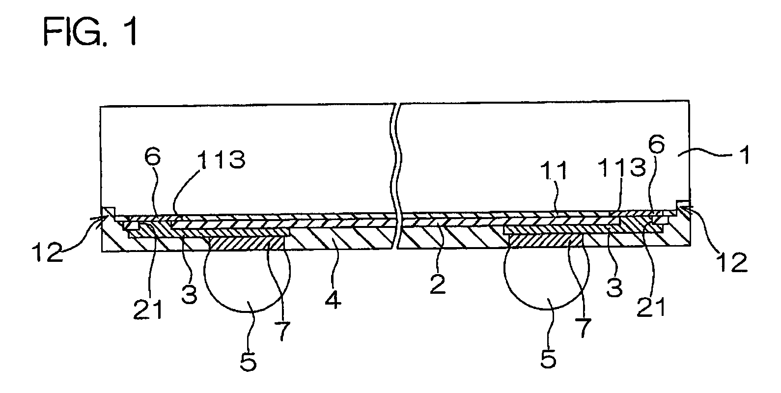
[0047]FIG. 1 is a sectional view illustrating the construction of a semiconductor device according to the present invention. The semiconductor device is a semiconductor device employing the WL-CSP technique, and includes a semiconductor chip 1, a passivation film (surface protection film) 11 covering a front surface of the semiconductor chip 1 (on a side formed with a functional device), a stress relieving layer 2 provided on the passivation film 11, rewirings 3 provided on the stress relieving layer 2, a sealing resin layer 4 provided over the rewirings 3, and metal balls 5 provided on the sealing resin layer 4.

[0048]The semiconductor chip 1 is of a rectangular shape as seen in plan, and has a groove 12 formed in a peripheral edge portion of the outermost front surface thereof. The formation of the groove 12 is achieved by cutting away a peripheral edge portion of the outermost front surface of the semiconductor chip 1 having, for example, a square sectional shape having a width of...

second embodiment

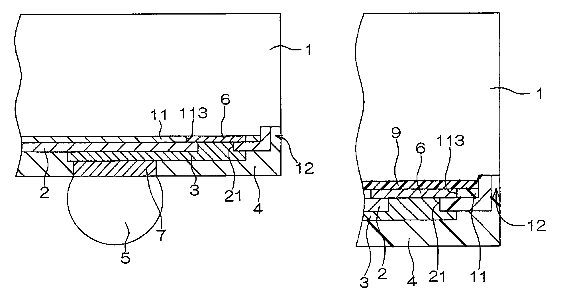
[0062]FIG. 3 is a sectional view illustrating the construction of a semiconductor device according to the present invention. In FIG. 3, components corresponding to those shown in FIG. 1 will be denoted by the same reference characters as in FIG. 1.

[0063]In the semiconductor device shown in FIG. 3, the semiconductor chip 1 is formed with no groove 12, and the side surfaces of the passivation film 11 are flush with the side surfaces of the stress relieving layer 2.

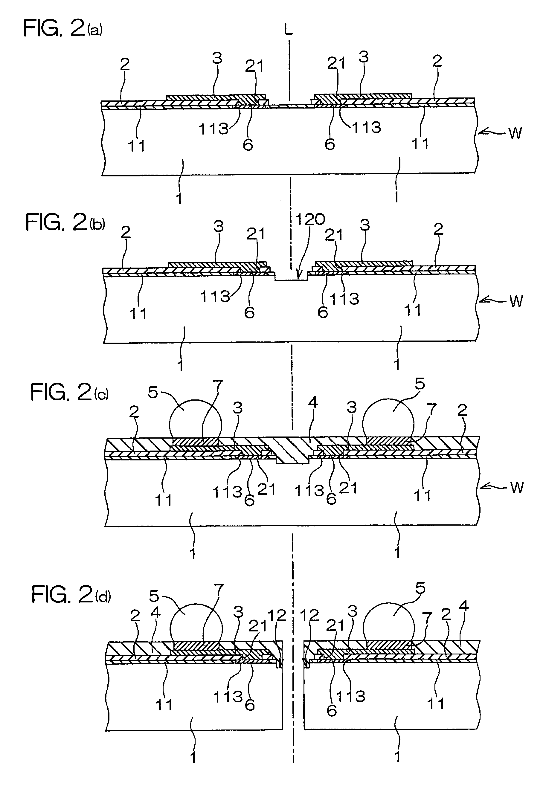
[0064]In a production process for the semiconductor device having such a construction, as shown in FIG. 4 (a), for example, a wafer W covered with a passivation film 11 is prepared, and stress relieving layers 2 and rewirings 3 are formed in this order on the passivation film 11. Thereafter, as shown in FIG. 4(b), a portion of the passivation film 11 exposed between the stress relieving layers 2 is etched away by using the stress relieving layers 2 as a mask. That is, a portion of the passivation film 11 present in a zone de...

third embodiment

[0067]FIG. 5 is a sectional view for explaining the construction of a semiconductor device according to the present invention. In FIG. 5, components corresponding to those shown in FIG. 1 will be denoted by the same reference characters as in FIG. 1.

[0068]In the semiconductor device shown in FIG. 5, the semiconductor chip 1 includes an interlayer film 9 such as of silicon oxide or silicon nitride provided between the electrode pads 6 (internal interconnection) formed in the front surface of the semiconductor chip 1 and a semiconductor substrate serving as a base of the semiconductor chip 1. The groove 12 extends to below the interlayer film 9 (into the semiconductor substrate), and the sealing resin layer 4 is partly disposed in the groove 12, whereby the side surfaces of the passivation film 11 and the interlayer film 9 are covered with the sealing resin layer 4.

[0069]With this arrangement, separation and cracking of the passivation film 11 and the interlayer film 9 can be prevente...


PUM


Abstract

An inventive semiconductor device includes a semiconductor chip having a passivation film, and a sealing resin layer provided over the passivation film for sealing a front side of the semiconductor chip. The sealing resin layer extends to a side surface of the passivation film to cover the side surface.

Description

TECHNICAL FIELD[0001]The present invention relates to a semiconductor device and a production method therefore and, particularly, to a semiconductor device and a production method therefore, which employ a WL-CSP (wafer level-chip scale package) technique.RELATED ART[0002]For higher performance and multifunctional semiconductor devices, the WL-CSP technique has recently been put into practical use. In the WL-CSP technique, the packaging of chips is completed on a wafer level, so that packages obtained by dicing the wafer each have a size equivalent to a chip size (for example, see Patent document 1).[0003]As shown in FIG. 19, a semiconductor device employing the WL-CSP technique includes a semiconductor chip 101 having a front surface entirely covered with a passivation film 102. The passivation film 102 has pad openings 104 through which parts of an internal interconnection provided in the front surface of the semiconductor chip 101 are exposed as electrode pads 103. A polyimide la...

Claims


Application Information

Patent Timeline
Patent Type & Authority Patents(United States)
IPC IPC(8): H01L23/48H01L23/52H01L29/40
CPCH01L23/3114H01L24/10H01L24/13H01L23/293H01L23/3171H01L23/562H01L2224/13099H01L2224/16H01L2924/01013H01L2924/01029H01L2924/01074H01L2924/3025H01L2924/01005H01L2924/01006H01L2924/01033H01L2924/014H01L2924/00H01L23/3178H01L23/3192H01L24/03H01L24/05H01L2224/02377H01L2224/0239H01L2224/05001H01L2224/05008H01L2224/05022H01L2224/05124H01L2224/05568H01L2224/05569H01L2224/05571H01L2224/05647H01L2224/13023H01L2224/131H01L2924/10161H01L2924/10253H01L2924/12042H01L2224/13H01L2924/00014H01L2924/00012H01L21/78H01L23/291H01L23/3142H01L23/528H01L23/544H01L24/02H01L24/94H01L24/96H01L2223/5446H01L2224/02255H01L2224/0226H01L2224/02381H01L2224/024H01L2224/12105H01L2224/13024H01L2224/13124H01L2924/05042H01L2924/05442H01L2924/0665H01L2924/07025H01L2924/182H01L2924/186
Inventor MIYATA, OSAMUKASAI, MASAKIHIGUCHI, SHINGO
Owner ROHM CO LTD
Why Eureka
Try Eureka