Interface circuit

a technology of interface circuits and circuits, applied in the field of interface circuits, can solve problems such as data destruction, data cannot be accurately taken, data cannot be read-in correctly, etc., and achieve the effect of simple circuit configuration

Inactive Publication Date: 2010-05-25
RENESAS ELECTRONICS CORP
View PDF8 Cites 26 Cited by
  • Summary
  • Abstract
  • Description
  • Claims
  • Application Information

AI Technical Summary

Benefits of technology

[0025]An object of the present invention is to provide an interface circuit that can reliably take in transfer data to produce internal read data with a simple circuit configuration.
[0028]According to the first aspect of the invention, the start of the preamble period is detected according to the data strobe signal and the delayed signal of the data strobe signal. According to a specification, the preamble period is determined to be in a range from 0.9 to 1.1 clock cycles. Therefore, by using the delay time that is close to and is shorter than the specification minimum value of the preamble period, the delayed data strobe signal and the data strobe signal take different logical values in the preamble period, and the start of the preamble period can be detected. Thus, by starting the operation of taking in the transfer data according to a detection signal thus obtained, the data can be taken in accurately. Even when the glitch noise occurs after the postamble period, the influence of the glitch noise can be prevented by completing the take-in of the data. Even when the glitch noise arrives during the next data transfer operation, the next data can be accurately taken in by resetting an operation caused by this glitch noise according to the correct detection of the preamble period, as far as the glitch noise arrives at the timing at which the completion of the preamble of this transfer data can be detected after the arrival of the glitch noise.
[0029]According to the second aspect of the invention, the first and second transfer circuits are employed as the transfer circuits each having FIFO circuits that alternately take in the transfer data, and the first and second transfer circuits are alternately activated in response to each data transfer instruction. Accordingly, in the case where the propagation delay of the transfer data is long, when the glitch noise occurs in the data strobe signal, the internal data can be produced by accurately taking in the data. Further, the two data transfer circuits are employed to be alternately activated, and therefore allow a longer delay in data propagation as compared with a configuration having only one data transfer circuit.

Problems solved by technology

Therefore, when the controller issues the data read instruction and takes in the transferred data at the same timing, the data cannot be accurately taken in.
When the flight time in data transfer from the memory increases, the glitch noise caused after this postamble adversely affects the next data read operation, resulting in a problem that next transfer data is destructed, and the data read from the memory cannot be correctly read-in in the controller.
In this case, the transfer data may be destruct upon being taken in due to the glitch noise.
Particularly, in the fast data transfer operation, a window (a period for which effective or valid data is transferred) of the data is short in time width, and a margin for data take-in timing is small, so that the glitch noise is more likely to destruct the data.
This results in increase in scale of the software or hardware.
When a plurality of memories are provided, since distances from the respective memories to the controller are different from each other, calibration must be performed for each memory, resulting in a problem that setting of the delay times takes a long time.
When the calibration is being performed, the data transfer cannot be performed, so that the process efficiency of the system lowers.
Therefore, in the circuit (flip-flop) producing internal read data of the data thus taken, a period of an enabled state overlaps with an active period of the clock signal only to a small extent, so that it may be impossible to take in the data accurately.
In this case, it may be impossible to detect accurately the effective data start timing for reading into data in the current data read operation.

Method used


Image

  • Interface circuit
  • Interface circuit
  • Interface circuit

Examples


first embodiment

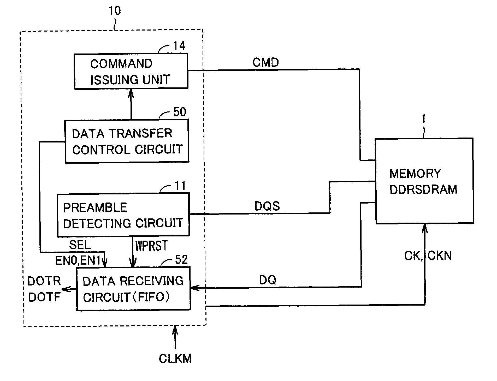
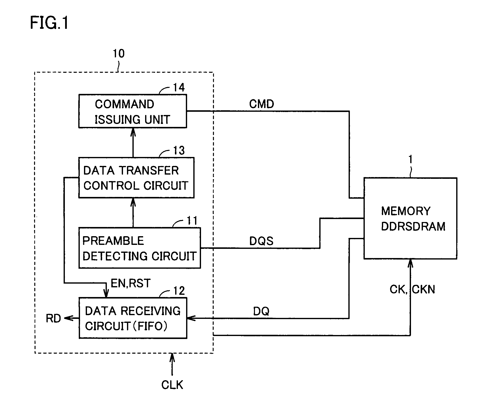
[0044]FIG. 1 shows an example of a construction of a processing system that has a controller with a memory interface circuit according to a first embodiment of the invention. The controller may be a memory controller or a processor. In the following description, the controller performs data transfer with an SDRAM, and is referred to as a “memory controller”.

[0045]In FIG. 1, the processing system includes a memory 1 and a memory controller 10 transferring data with memory 1. Memory controller 10 receives a clock signal CLK, and has an operation cycle defined according to clock signal CLK. Memory 1 is formed of, e.g., a DDR SDRAM, and transfers read data DQ to memory controller 10 together with a data strobe signal DQS in synchronization with clock signals CK and CKN when a command CMD issued from memory controller 10 instructs a read mode. Clock signals CK and CKN are complementary to each other, and are applied from memory controller 10.

[0046]Memory controller 10 includes a data rec...

second embodiment

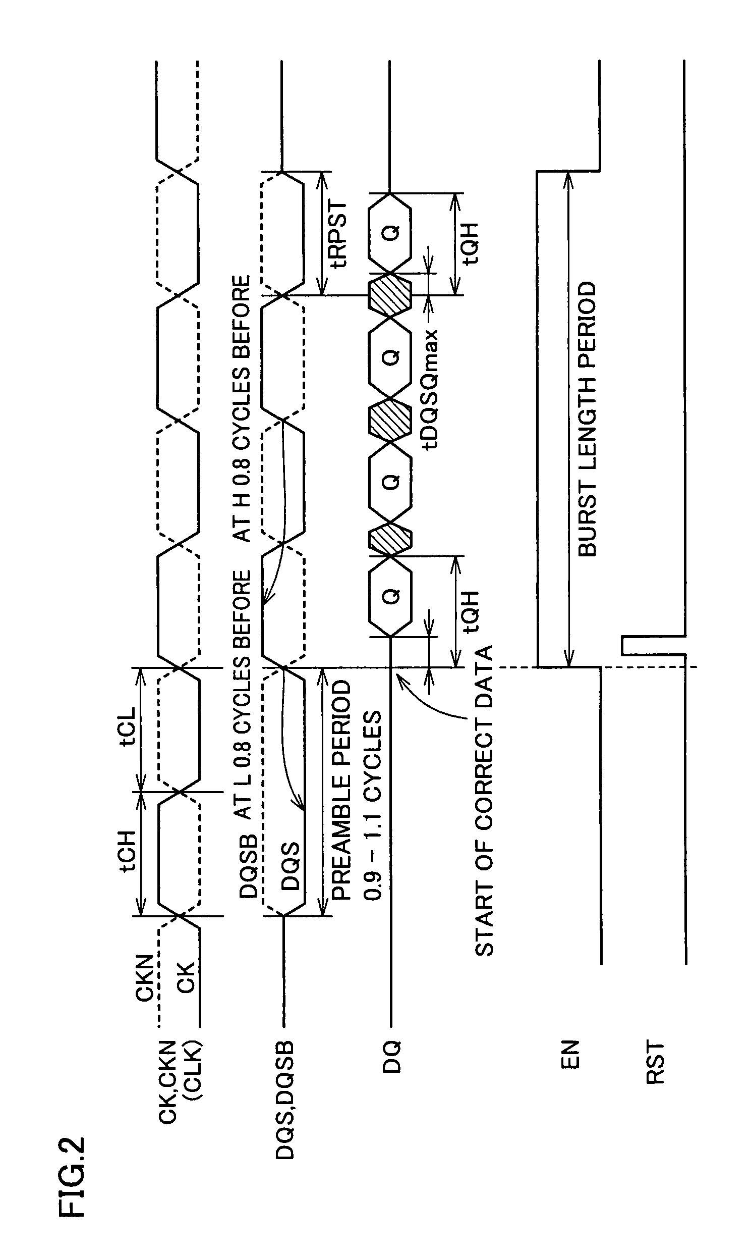
[0075]FIG. 5 schematically shows an example of a configuration of data receiving circuit 12 according to a second embodiment of the invention. In the second embodiment shown in FIG. 5, an output signal of preamble detecting circuit 11 is used as write pointer reset signal WPRST. This preamble detecting circuit 11 has the same configuration as preamble detecting circuit 11 shown in FIG. 3, but uses detection signal DKT of detector 22 shown in FIG. 3 as write pointer reset signal WPRST instead of the reset signal applied from reset signal generating circuit 24 shown in FIG. 3. This write pointer reset signal WPRST resets a write pointer indicating a write address of the FIFO circuits included in data receiving circuit 12 to an initial value.

[0076]Data receiving circuit 12 includes delay circuits 30-33 as a transfer clock signal generating circuit. Delay circuit 30 delays data strobe signal DQS applied from the memory by ¼ phase (90 degrees). Delay circuit 31 further delays a ¼ phase d...


PUM


Abstract

A variable delay line receives and delays a data strobe signal transferred from a data source side in synchronization with a transfer data by a predetermined period, and produces a delayed data strobe signal and the non-delayed data strobe signal to a detector. The detector determines that a preamble period ends and effective data is transferred, when the delayed data strobe signal is at the L level at the time of rising of the non-delayed data strobe signal from the L level to the H level. According to a result of detection, an interface circuit unit takes in the transfer data and initializes a take-in address. The data strobe signal changes to a high-impedance state when a postamble ends. An influence of a glitch noise is avoided upon this change of the data strobe signal, and the data transfer can be executed fast and accurately.

Description

BACKGROUND OF THE INVENTION[0001]1. Field of the Invention[0002]The present invention relates to an interface circuit for receiving data transferred from a source side, and particularly to a configuration of an interface circuit that receives data transferred in synchronization with a data strobe signal from a memory. More particularly, the present invention relates to a configuration for detecting a transfer mode in a memory interface circuit receiving data from a memory transferring the data in a Double Data Rate (DDR) mode in which the data is transferred in synchronization with rising and falling of a clock signal.[0003]2. Description of the Background Art[0004]For achieving fast data transfer, SDRAMs (Synchronous Dynamic Random Access Memories) that transfer data in synchronization with a clock signal have been widely and generally used. A Double Data Rate mode (DDR mode) in which the data is transferred in synchronization with rising and falling of the clock signal is employed...

Claims


Application Information

Patent Timeline
Patent Type & Authority Patents(United States)
IPC IPC(8): G11C8/00
CPCG11C8/08G11C7/1066
Inventor OSAWA, TOKUYAHARAGUCHI, MASARUMOROOKA, YOSHIKAZUKINOSHITA, HIROSHI
Owner RENESAS ELECTRONICS CORP
Why Eureka
Try Eureka