Device and method for signal processing

a signal processing and signal processor technology, applied in the field of devices and methods for signal processing, can solve the problems of rare use, inability to simultaneously perform several complicated mathematical operations, and practically inability of digital signal processors to achieve the effect of facilitating signal processing, low cost and easy integration with other integrated devices

Active Publication Date: 2010-06-08
NOVATRANS GRP SA
View PDF7 Cites 0 Cited by
  • Summary
  • Abstract
  • Description
  • Claims
  • Application Information

AI Technical Summary

Benefits of technology

[0005]There is a need in the art to facilitate signal processing, such as transformation or correlation, by providing a novel technique capable of performing analog real-time signal processing, which can be implemented in a low cost dedicated chip (or as part of another chip like DSP) and which can easily be integrated with other integrated devices.
[0009]It should also be understood that the accuracy of the approximation depends on the linearity of the I-V curve resulting from the electrodes' arrangement (and possibly also of a light modulator as the case may be). The invention also provides for the device configuration aimed at improving the linearity.
[0014]The Photocathode as well as Anode may be made of metal or semiconductor materials. The Photocathode is preferably a reduced work function electrode. Negative electron affinity (NEA) materials can be used (e.g., diamond), thus reducing the photon energy (exciting energy) necessary to induce photoemission in the Photocathode. Another way to reduce the work function is by coating or doping the Photocathode with an organic or inorganic material that reduces the work function. For example, this may be metal, multi-alkaline, bi-alkaline, or any NEA material, or GaAs electrode with cesium coating or doping thereby obtaining a work function of about 1-2 eV. The organic or inorganic coating also serves to protect the cathode electrode from contamination. A gap between the Photocathode and Anode may be a vacuum gap; or may be a gas-medium gap (e.g., air) in which case the gas pressure in the gap is sufficiently low to ensure that a mean free path of electrons accelerating from the Photocathode to the Anode is larger than a distance between them (larger than the gap length). Accommodating the Photocathode and Anode with such an appropriate distance between them allows for eliminating the need for vacuum between them or at least significantly reducing the vacuum requirements. For example, for a 10 micron gap between Photocathode and Anode, the gas pressure of a few mBar may be used.
[0020]The present invention provides for the correlation suitable to be used for these purposes. This may for example be implemented by setting a lot of different variations of the string to be found in different units of an array of triodes, thus obtaining a very efficient processing. The Gates of triodes are set to reflect the string to be looked for, and the other input signal (light signal) is indicative of the part of the genome where the string is looked for.
[0026]Preferably, the input signal to be processed is the light signal, and accordingly all the Photocathodes are irradiated with the same photon flux. This facilitates synchronization of processing.
[0032]the device thereby providing an output signal at the Anode in the form of approximation of a product, x(t)·y(t), thereby enabling extraction of the required signal from the input signal.

Problems solved by technology

However, digital signal processors are practically incapable of concurrently performing several complicated mathematical operations.
For example, Fourier transform, which is in principle very useful, is actually rarely used because of its significant resource consumption and low-speed operation.

Method used


Image

  • Device and method for signal processing
  • Device and method for signal processing
  • Device and method for signal processing

Examples


Embodiment Construction

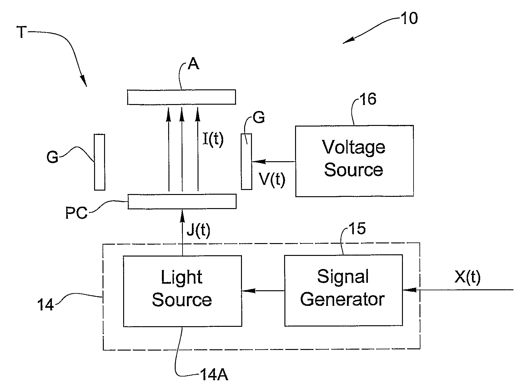
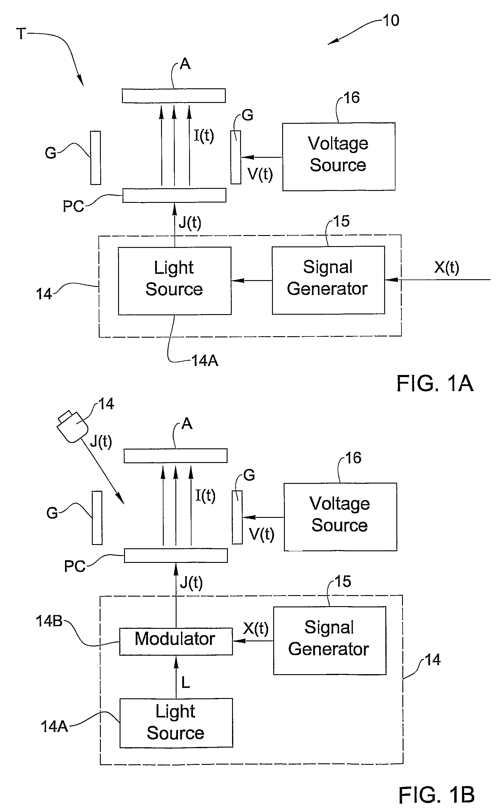
[0046]Referring to FIGS. 1A and 1B, there are schematically illustrated two examples of a basic unit 10 of an analog real-time signal processing device of the present invention. The device is configured and operable to provide electrical mathematical transformation of functions (or signals).

[0047]In the present example, the device 10 is configured as a triode (e.g., transistor) T including a Photocathode PC, an anode A, and a Gate G (which is formed by two spaced-apart electrodes that are electrically connected together) between the Photocathode and Anode. The Photocathode PC is exposed to a photon flux J(t) being a function of an input signal x(t).

[0048]In the present example of FIG. 1A, this is implemented using an illuminating assembly 14 including a light source system 14A and a signal generator 15. The signal generator 15 receives an input signal x(t), and operates the light source system 14A to generate the corresponding photon flux J(t).

[0049]In FIG. 1B, the same is achieved ...


PUM


Abstract

An analog real-time signal processing device and method are presented. The device is configured to perform electrical signal processing. The device comprises an electronic circuit including at least one basic unit of electrodes, the basic unit being configured to be sensitive to an external field, such as input photon flux, indicative of a first input signal to cause emission of charged particles and configured to define at least one electrical input for a second input signal and one electrical output, thereby providing the electrical output in the form of an approximation of a product of the first and second input signals.

Description

FIELD OF THE INVENTION[0001]This invention relates to a device and method for signal processing, such as signal transformation, correlation, etc.BACKGROUND OF THE INVENTION[0002]Most of the known techniques for mathematical transformation of functions (or signals) utilize digital signal processing. The main advantage of using digital signal processing is the flexibility to change the way the signal is processed at any time and very quickly; digital signal processors are relatively cheap and easy to use.[0003]However, digital signal processors are practically incapable of concurrently performing several complicated mathematical operations. For example, Fourier transform, which is in principle very useful, is actually rarely used because of its significant resource consumption and low-speed operation. In reality, other “tricks” are used in order to avoid such transformation, thus getting a very similar result through far less operations (for example correlation with a few tones to fin...

Claims


Application Information

Patent Timeline
Patent Type & Authority Patents(United States)
IPC IPC(8): G06G7/16H01L31/0352
CPCG06E3/005H01J21/02H01J1/34
Inventor HALAHMI, EREZDIAMANT, GILADSHVARTS, DIMITRYNAAMAN, RONKRONIK, LEEOR
Owner NOVATRANS GRP SA
Why Eureka
Try Eureka