Noise-reducing transistor arrangement

a transistor and noise reduction technology, applied in the field of noise reduction transistor arrangement, an integrated circuit, can solve the problems of limited performance of analog circuits, limited accuracy of electrical circuits, and low-frequency noise of mos transistors

Inactive Publication Date: 2010-06-08
INFINEON TECH AG
View PDF8 Cites 52 Cited by
  • Summary
  • Abstract
  • Description
  • Claims
  • Application Information

AI Technical Summary

Problems solved by technology

The noise of a field effect transistor (in particular MOSFET, “metal oxide semiconductor field effect transistor”) limits the accuracy of an electrical circuit.
This is problematic particularly when a signal having a small amplitude occurs in such a circuit.
Therefore, the performance of an analog circuit, in particular, is limited by the phenomenon of noise.
The low-frequency noise of a MOS transistor is caused by statistical loading or unloading of defect states in particular at the interface between the channel region and the gate insulating region of the field effect transistor.
Predominantly those defects whose energy level lies close to the (quasi) Fermi level of the charge carriers contributing to the current flow contribute to the low-frequency noise.
However, narrow limits are imposed on the technological optimization possibilities.
What is disadvantageous about this method, however, is the restriction of the degrees of freedom in the circuit design from other standpoints, such as e.g. power consumption, modulation range, bandwidth.
Furthermore, the noise reduction that can be achieved by means of this method is small.
One disadvantage of this method is the increased area taken up.
Moreover, an increased power consumption may result, particularly if the bandwidth of the circuit cannot be reduced, since then only the widths, but not the lengths of the transistors are permitted to be increased.
“Reducing MOSFET 1 / f Noise and Power Consumption by Switched Biasing” IEEE Journal of Solid-State Circuits Vol. 35, No. 7, pages 994 to 1001, 2000, is restricted, however, to circuits in which the transistors are periodically switched on and off.
This is not desirable, however, particularly in many analog circuits since continuous signals are intended to be processed.
One problem of SOI field effect transistors is the floating body effect inherent to them, which leads to a kink effect in the case of the drain current.
The increase in the substrate potential leads to a reduction of the threshold voltage and results in a kink in the output characteristic curve or characteristic, as a result of which the gain of analog amplifiers and the constancy of current sources are impaired.
This results from the poor thermal conductivity of the buried silicon oxide layer arranged beneath a silicon layer of an SOI substrate, so that the channel temperature of the SOI device may rise by tens of ° C. above the temperature at normal operation.
The insulating substrate forms a thermal barrier, so that the heat generated by the operated device cannot simply be transferred to the substrate.
The output conductivity can be low or even negative at low frequencies and can then rise with the frequency, which leads to unforeseen gain and phase variations.
Interacting devices that adjoin one another may be at different temperatures, which may lead to a thermally induced mismatch.
The temperature gradients which result from the self-heating effect and the thermal coupling effect lead to non-isothermal conditions and therefore to malfunctions, see Tenbroek et al.
The body potential in a partially depleted SOI transistor is kept constant by the body contact, although the problem occurs as to how the system configuration can be optimized given simultaneous minimization of the effect of stray resistance and stray capacitance between the body contact path and the active region.
In particular, the physical definition of the contact to the FinFET or to the planar double gate transistor requires tricky lithography.
However, even fully depleted device structures cannot prevent self-heating effects, and it is necessary to take account of the small process margin of FD devices with regard to the threshold voltage control, and also a loss of area.
Furthermore, the high inherent body resistance and the high inherent body capacitance which are introduced by the body contact are problematic, and the floating body effects are far more serious in an analog design.
Even advanced double and triple gate concepts suffer from self-heating and, depending on how they are constructed, they may also be exposed to charge accumulation effects such as the kink effect in partially depleted SOI substrates.

Method used


Image

  • Noise-reducing transistor arrangement
  • Noise-reducing transistor arrangement
  • Noise-reducing transistor arrangement

Examples


Embodiment Construction

[0049]The invention is based on the problem of effectively reducing the low-frequency noise of transistors with little outlay.

[0050]The problem is solved by means of a noise-reducing transistor arrangement, by means of an integrated circuit, and by means of a method for reducing the noise of field effect transistors.

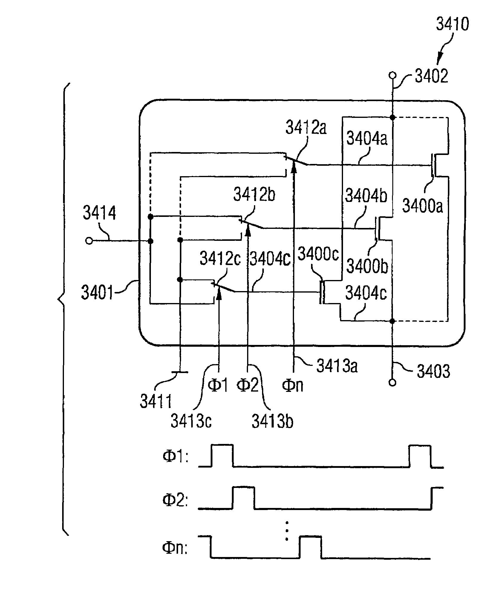
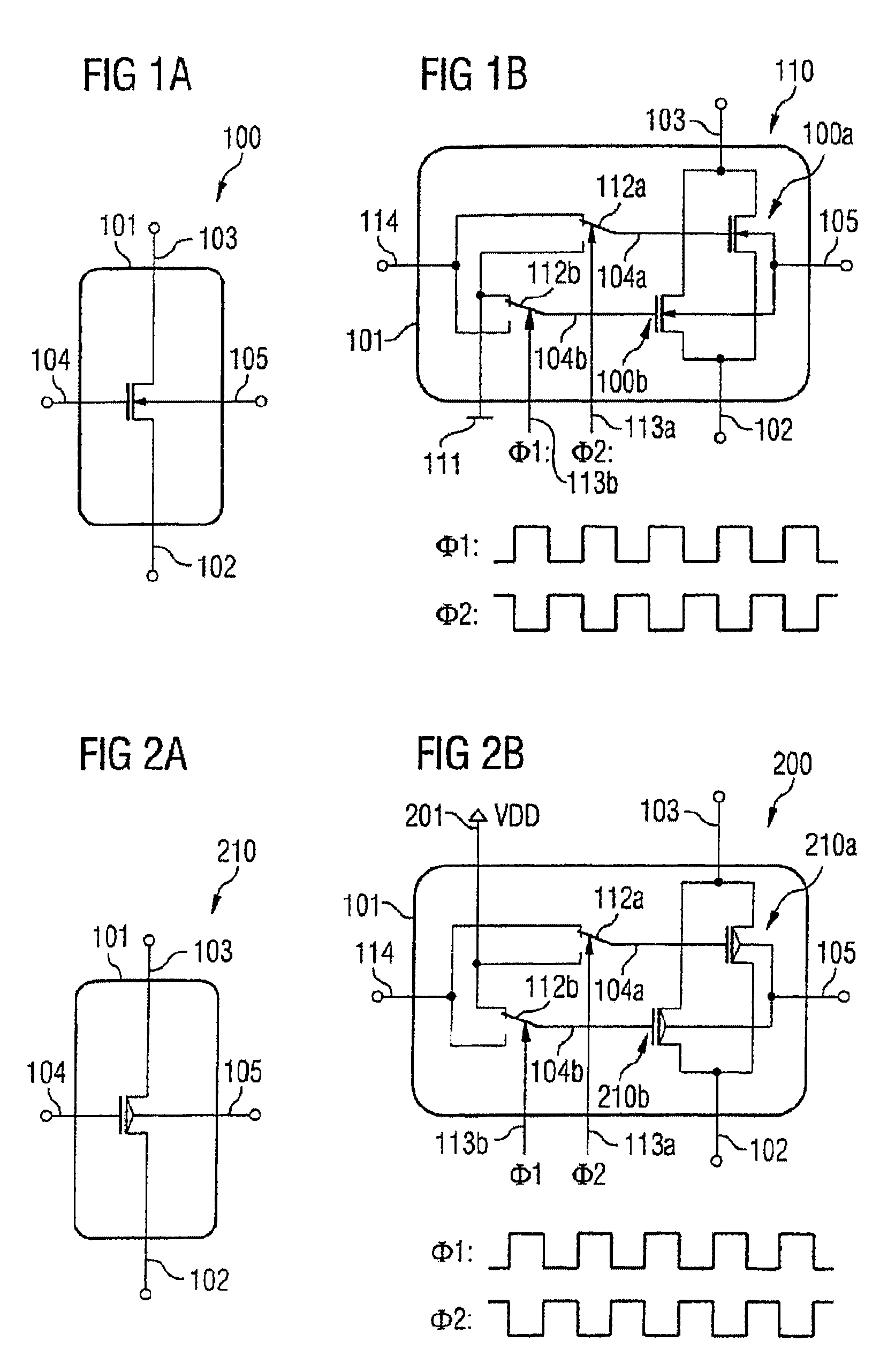
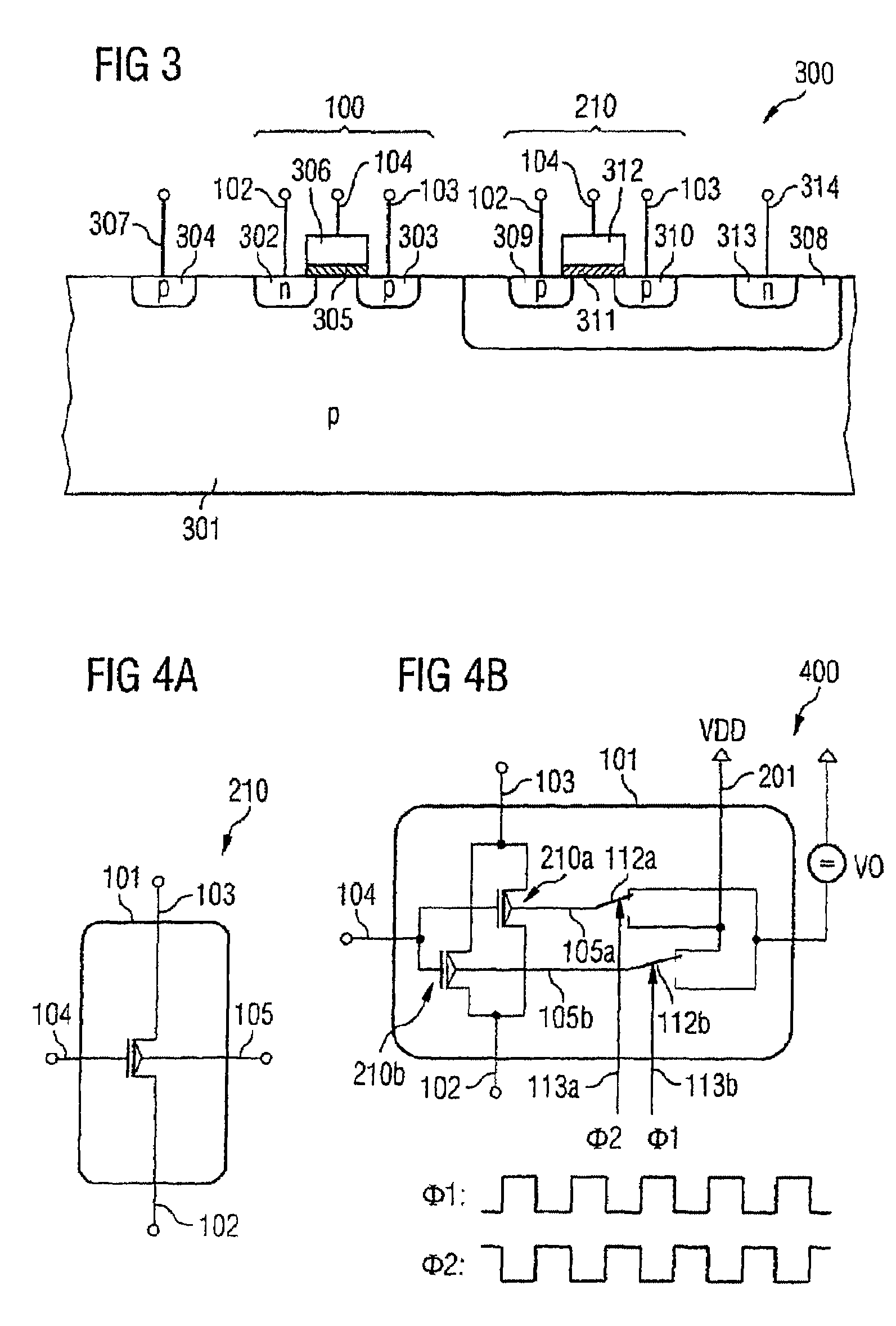
[0051]The noise-reducing transistor arrangement according to the invention has a first and a second field effect transistor, each of which has a first source / drain terminal (source terminal) and a second source / drain terminal (drain terminal) and a control terminal for application of a first and a second signal. The first source / drain terminals of the first and second field effect transistors are coupled to one another. The second source / drain terminals of the first and second field effect transistors are coupled to one another. The transistor arrangement is set up in such a way that alternately the first signal can be applied to the control terminal of the first field e...


PUM


Abstract

Noise-reducing transistor arrangement having first and second field effect transistors (FETs) having source terminals coupled together, drain terminals coupled together, and control terminals for application of a first or second signal. A clock generator unit is configured to provide the first and second signals alternately to the FETs with an alternating frequency which is at least as great as the cut-off frequency of the noise characteristic of the FETs, or with a reciprocal alternating frequency which is less than a mean lifetime of an occupation state of a defect in the boundary region between channel region and gate insulating layer of the FETs. The first signal is applied to the control terminal of the first FET and, simultaneously, the second signal to the control terminal of the second FET. The second signal is applied to the control terminal of the first FET and, simultaneously, the first signal to the control terminal of the second FET.

Description

CROSS-REFERENCE TO RELATED APPLICATION[0001]This application is a nation stage of International Patent Application Serial No. PCT / DE2004 / 002657, filed Dec. 3, 2004, which published in German on Jun. 30, 2005 as WO / 2005 / 060099, and is incorporated herein by reference in its entirety.FIELD OF THE INVENTION[0002]The invention relates to a noise-reducing transistor arrangement, an integrated circuit, and a method for reducing the noise of field effect transistors.BACKGROUND OF THE INVENTION[0003]The noise of a field effect transistor (in particular MOSFET, “metal oxide semiconductor field effect transistor”) limits the accuracy of an electrical circuit. This is problematic particularly when a signal having a small amplitude occurs in such a circuit. Therefore, the performance of an analog circuit, in particular, is limited by the phenomenon of noise.[0004]The low-frequency noise of a MOS transistor is caused by statistical loading or unloading of defect states in particular at the inter...

Claims


Application Information

Patent Timeline
Patent Type & Authority Patents(United States)
IPC IPC(8): H03K17/687H03K17/16
CPCH03K17/162H01L2924/0002H01L2924/00
Inventor BREDERLOW, RALFKOH, JEONGWOOKPACHA, CHRISTIANTHEWES, ROLAND
Owner INFINEON TECH AG
Why Eureka
Try Eureka