Silicon-on insulator substrate and method for manufacturing the same

a technology of silicon-on-insulator substrate and substrate, which is applied in the direction of individual semiconductor device testing, semiconductor/solid-state device testing/measurement, instruments, etc., can solve the problems of degrading the in-plane uniformity, affecting the uniformity of the active layer, and damage to the active layer, so as to reduce the variation of the active layer thickness, remove the crystal defect layer, and the active layer thickness is more uniform

Inactive Publication Date: 2010-06-15
SUMCO CORP
View PDF14 Cites 6 Cited by
  • Summary
  • Abstract
  • Description
  • Claims
  • Application Information

AI Technical Summary

Benefits of technology

[0018]In accordance with the present invention, because the oxide film is formed only in the active layer, and because the active layer is formed with a thickness of 10 to 200 nm and a thickness variation throughout the active layer of 1.5 nm or less by selectively using only the reactive radicals generated by a plasma etching process to etch a surface of the active layer, it is possible to reduce the variation in the active layer thickness and make the active layer thickness more uniform without damaging the surface of the active layer.
[0019]Also, hydrogen ions are implanted from the surface of an active layer-forming substrate on at least the surface of which an oxide film has been formed, thereby creating an ion-implanted region within the active layer-forming substrate; a bonded substrate is produced by subjecting the active layer-forming substrate to a first heat treatment in a state in which the active layer-forming substrate contact, through the oxide film, with a base substrate, so as to split the active layer-forming substrate from the base substrate at the ion-implanted region and form an active layer on a surface of the base substrate; film thickness measurements are taken throughout the active layer; only reactive radicals generated by a plasma etching process are selectively used to etch the surface of the active layer and thereby thin the active layer to a predetermined thickness; and then the bonded substrate is subjected to a second heat treatment. In this way, it is possible to both remove the crystal defect layer at the surface of the active layer and also to reduce the thickness variation in the active layer so as to provide a more uniform active layer thickness without damaging the surface of the active layer.
[0020]Moreover, by adding to the above etching process, a step in which, regardless of the active layer thickness measurement data, a boundary area between an inactive region and an active region at the periphery of the bonded substrate is additionally plasma-etched, the boundary line between the inactive region and the active region can be rendered smooth without increasing the number of processing operations. As a result, particle generation can be suppressed.

Problems solved by technology

Because these reactive ions are used as part of the etchant for etching the surface of the active layer, they end up causing damage to the active layer.
As for the CMP method and the sacrificial oxidation method, because both processes thin the entire surface at the same time, they cannot improve the in-plane uniformity in the thickness of the active layer.
Also, the amount of thinning is not everywhere uniform in-plane, there being some variation in the initial in-plane thickness, which may have the opposite effect of degrading the in-plane uniformity.

Method used


Image

  • Silicon-on insulator substrate and method for manufacturing the same
  • Silicon-on insulator substrate and method for manufacturing the same
  • Silicon-on insulator substrate and method for manufacturing the same

Examples


example 1

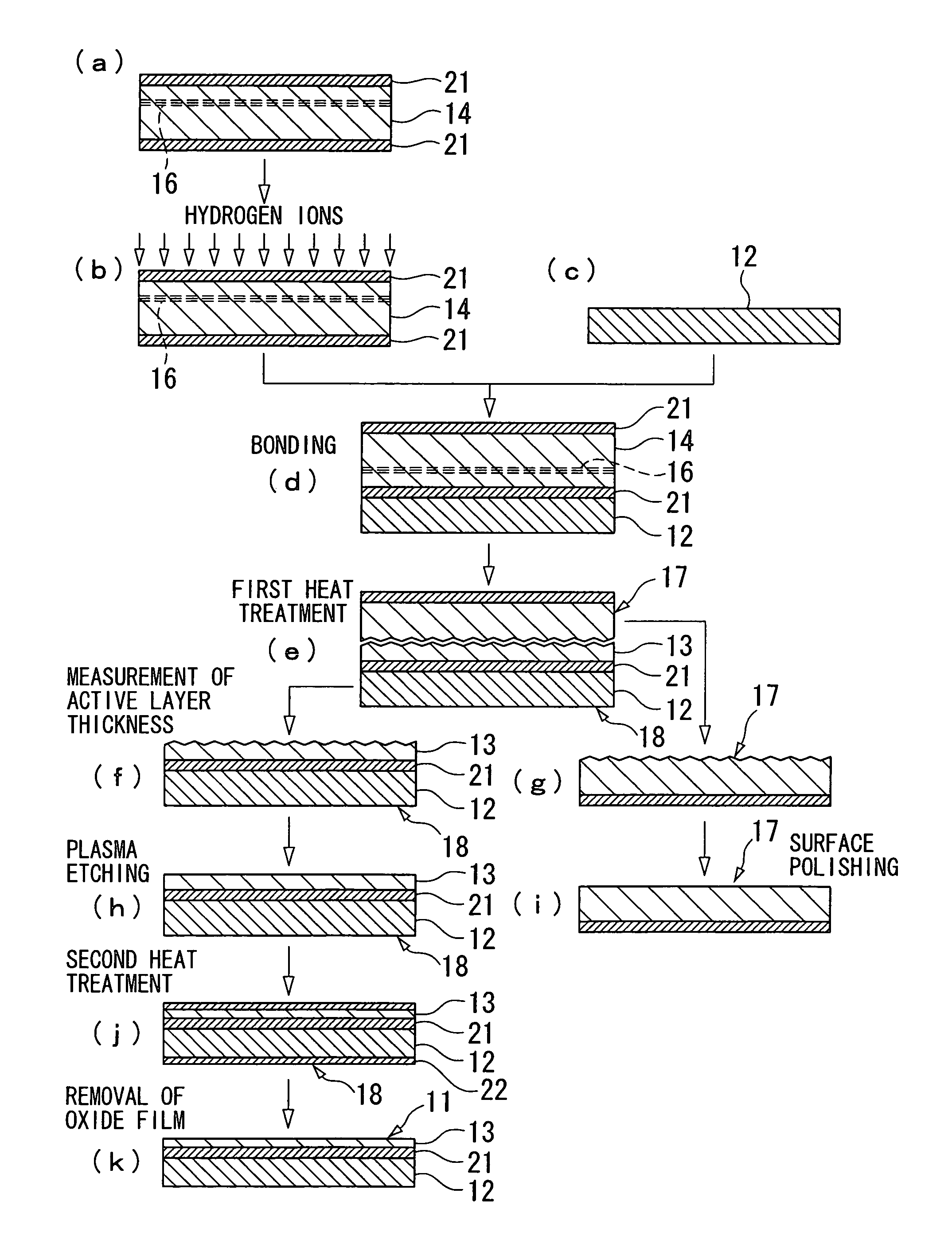
[0043]As shown in FIG. 1, first an active layer-forming substrate 14 made of a single-crystal silicon wafer and having a diameter and thickness of 200 mm and 0.725 mm, respectively, was held in an oxygen atmosphere at 1000° C. for 5 hours so as to carry out a heat treatment; thereby a first oxide film 21 was formed not only in the top side of the active-forming substrate 14, but also in the back side and lateral face thereof. This first oxide film 21 had a thickness of about 150 nm. Next, hydrogen ions were implanted at a dose of 6×10¹⁶ / cm2 and an acceleration energy of 50 keV from the surface of the active layer-forming substrate 14; thereby an ion-implanted region 16 was formed within the active layer-forming substrate 14 (FIG. 1(b)). The depth (implantation peak position) of this ion-implanted region 16 was set to about 500 nm, including the above first oxide film 21. A base substrate 12 which was made of a single-crystal silicon wafer and which had the same surface area as the a...


PUM


Abstract

This SOI substrate includes a base substrate which includes a single-crystal semiconductor and an active layer which includes a single-crystal semiconductor and is bonded to the base substrate with an oxide film therebetween. The oxide film is formed only in the active layer. The active layer is formed with a thickness of 10 to 200 nm and a thickness variation throughout the active layer of 1.5 nm or less by etching a surface of the active layer while selectively using only the reactive radicals generated by a plasma etching process.

Description

TECHNICAL FIELD[0001]The present invention relates to a silicon-on-insulator (SOI) substrate which includes an oxide layer produced using a hydrogen ion implantation technique and an active layer provided on the oxide layer. The present invention also relates to a method for manufacturing such an SOI substrate.[0002]This application claims priority from Japanese Patent Application No. 2004-159398, filed on May 28, 2004, the content of which is incorporated herein by reference.BACKGROUND ART[0003]A method for manufacturing SOI wafers has hitherto been disclosed in which, first, an oxide film is formed on at least one of two silicon wafers and a microbubble layer (trap layer) is formed at the interior of one of the silicon wafers by implanting hydrogen ions or rare-gas ions from the upper surface of the wafer. Next, the ion implanted surface of this wafer is brought into contact with the other wafer such that the oxide film is disposed therebetween, then heat treatment is applied; the...

Claims


Application Information

Patent Timeline
Patent Type & Authority Patents(United States)
IPC IPC(8): H01L21/30H01L21/02H01L21/3065H01L21/762H01L27/12
CPCH01L21/3065H01L21/76254Y10T428/24479
Inventor MORITA, ETSUROUSANO, RITAROUENDO, AKIHIKO
Owner SUMCO CORP
Why Eureka
Try Eureka