Epoxy resin composition and semiconductor device

a technology of epoxy resin and semiconductor elements, applied in semiconductor devices, semiconductor device details, solid-state devices, etc., can solve the problems of affecting the reliability of the semiconductor device, the semiconductor device is subjected to a higher temperature environment, and the epoxy resin composition is required. , to achieve the effect of excellent adhesion, excellent adhesion and excellent solder reflow resistan

Inactive Publication Date: 2010-06-22
SUMITOMO BAKELITE CO LTD
View PDF21 Cites 7 Cited by
  • Summary
  • Abstract
  • Description
  • Claims
  • Application Information

AI Technical Summary

Benefits of technology

[0013]A second object of the present invention is, in addition to attaining the above-stated first object, to provide an epoxy resin composition for encapsulating a semiconductor further having an excellent productivity, and a semiconductor device using the same for encapsulating a semiconductor element.
[0014]A third object of the present invention is, in addition to attaining the above-stated first object, to provide an epoxy resin composition for encapsulating a semiconductor having an excellent flowability, and a semiconductor device using the same for encapsulating a semiconductor element having a high reliability.
[0051]According to the first aspect of the present invention, the epoxy resin composition for encapsulating a semiconductor which has a flame resistance grade of V-0 of UL-94 without using a halogen based flame retardant, an antimony compound or other flame retarders, is excellent in adhesion with various substrates such as a semiconductor element, a lead frame or the like, particularly an adhesion with a preplating frame of Ni, Ni—Pd, Ni—Pd—Au or the like, and has an excellent solder reflow resistance to the extent that crack or delamination with the substrate does not occur in a semiconductor device upon solder processing after absorption of moisture, and a semiconductor device wherein a semiconductor element is encapsulated with the use of the epoxy resin composition can be obtained.
[0052]According to the second aspect of the present invention, the epoxy resin composition for encapsulating a semiconductor which has a flame resistance grade of V-0 of UL-94 without using a halogen based flame retardant, an antimony compound or other flame retarders, is excellent in adhesion with various substrates such as a semiconductor element, a lead frame or the like, particularly an adhesion with a preplating frame of Ni, Ni—Pd, Ni—Pd—Au or the like by adding a triazole compound to the epoxy resin composition, has an excellent solder reflow resistance to the extent that crack or delamination with the substrate does not occur in a semiconductor device upon solder processing after absorption of moisture, and further can solve problems of releasing property, continuous moldability, appearance of a molded article and soling of a mold or the like, and a semiconductor device wherein a semiconductor element is encapsulated with the use of the epoxy resin composition can be obtained.
[0053]According to the third aspect of the present invention, the epoxy resin composition for encapsulating a semiconductor which has a flame resistance grade of V-0 of UL-94 without using a halogen based flame retardant, an antimony compound or other flame retarders, and has high solder reflow resistance which can be used for a lead-free solder without declining flowability, and a semiconductor device which having high reliability wherein a semiconductor element is encapsulated with the use of the epoxy resin composition can be obtained with high productivity.

Problems solved by technology

In the circumstances, a demand for the epoxy resin composition for encapsulating a semiconductor element is increasing severe.
Thereby, the semiconductor device is subjected to a higher temperature environment than ever, which is apt to cause a defect greatly detracting the reliability of the semiconductor device such as delamination at an interface between a semiconductor element or a lead frame and a cured product of the epoxy resin composition, or a crack in the semiconductor device.
However, such plating has a problem of notably poor adhesion with a cured product of the epoxy resin composition, which may cause delamination at the interface when mounting on a surface.
However, this method has a problem that a large amount of the metal hydroxide is required to obtain an expected flame retardant effect.
Additionally, if the compound ratio of the metal hydroxide is increased to obtain a sufficient flame resistance, the flowability and curability of the epoxy resin composition during molding are decreased, and the mechanical strength of the cured product is deteriorated.
As a result, the solder reflow resistance is deteriorated in the temperature range of mounting the lead-free solder.
However, such an epoxy resin composition does not have a sufficient flame resistance and thereby requires addition of a flame retardant.
Additionally, such an epoxy resin composition exhibits a low adhesion to the preplating frame.
Thereby, the reliability is low, particularly in a package using such a preplating frame.
Furthermore, such an epoxy resin composition has a low crosslinking density and thereby a molded article immediately after curing is so soft that a problem may arise in a continuous molding process such as an insufficient release of the resin from the mold, which may reduce productivity.
In this case, the adhesion is deteriorated.
Although a silicone oil having a polyether chain greatly contributes to improvement of productivity, the solder reflow resistance is deteriorated because of increased moisture absorption due to the polyether chain.
However, if a compounding ratio of an inorganic filler is increased in order to apply for a case of using a lead-free solder, a sufficient flowability cannot be obtained, which prevents the realization of this method.

Method used


Image

  • Epoxy resin composition and semiconductor device
  • Epoxy resin composition and semiconductor device
  • Epoxy resin composition and semiconductor device

Examples


examples

[0120]Examples of the present invention are hereinafter described. The scope of the present invention is not restricted by these examples. The compounding ratio is expressed by “part by weight”.

[0121]Hereinafter, Example series (1) is regarding the first aspect, Example series (2) is regarding the second aspect and Example series (3) is regarding the third aspect.

Example Series (1)

Example (1)-1

[0122]The following components were mixed with each other by means of a mixer, and thereafter the mixture was mixed and kneaded by means of two rolls having a surface temperature of 95° C. and 25° C. respectively. Then, the mixture was cooled and grinded to obtain an epoxy resin composition. Properties of the obtained epoxy resin composition were evaluated in the following manner. The evaluation results are shown in Table 1.

[0123]Epoxy resin 1: an epoxy resin represented by the following formula (1a) (softening point 44° C., epoxy equivalent 234, hereafter referred as “E-1”) 6.21 parts by weig...

example series (

3)

Example (3)-1

[0205]The following components were mixed with each other by means of a mixer, and thereafter the mixture was mixed and kneaded by means of two rolls having a surface temperature of 95° C. and 25° C. respectively. Then, the mixture was cooled and grinded to obtain an epoxy resin composition. Properties of the obtained epoxy resin composition were evaluated in the following manner. The evaluation results are shown in Table 7.

[0206]Epoxy resin 1: an epoxy resin represented by the following formula (1a) (softening point 44° C., epoxy equivalent 234) 6.42 parts by weight
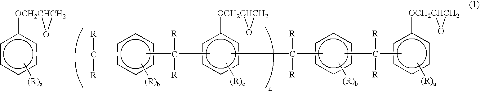
Formula (1a)

[0207]

[0208]Phenolic resin 1: a phenolic resin represented by the following formula (2a) (softening point 107° C., hydroxyl group equivalent 198) 4.28 parts by weight
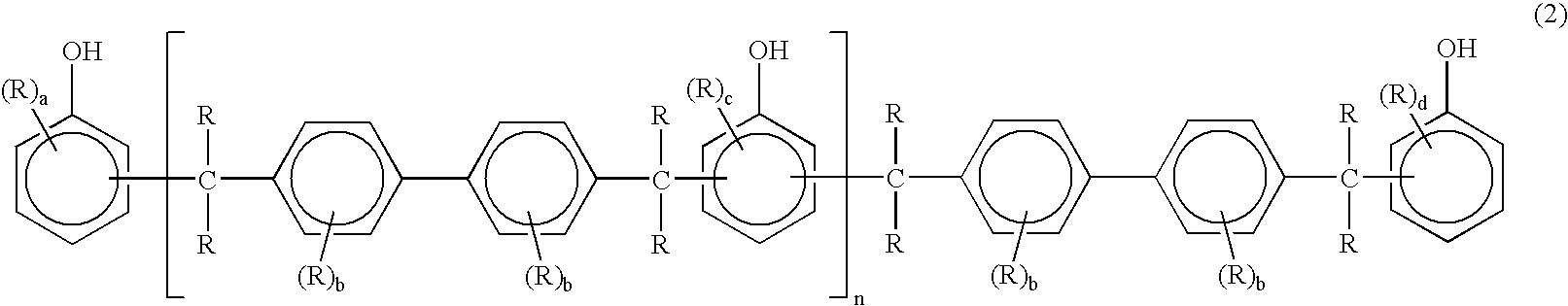
Formula (2a)

[0209]

[0210]Curing accelerator 1: a curing accelerator represented by the following formula (5a) 0.20 parts by weight

Formula (5a)

[0211]

wherein, M=1.

[0212]

Silane coupling agent 1: γ-0.20 parts by weightmercaptotripropylm...


PUM

PropertyMeasurementUnit
wt %aaaaaaaaaa
softening pointaaaaaaaaaa

Abstract

The present invention is to provide an epoxy resin composition for encapsulating a semiconductor having a high flame resistance without using a flame retarder and having an excellent solder reflow resistance, and a semiconductor device using the same for encapsulating a semiconductor element. An epoxy resin composition for encapsulating a semiconductor of each of the first, second and third aspects essentially comprises (A) a phenol aralkyl type epoxy resin having a phenylene structure, (B) a phenol aralkyl type phenolic resin having a biphenylene structure and (D) an inorganic filler as common components, wherein (D) the inorganic filler is contained at the rate of 84 wt % or more and 92 wt % or less of the total amount of the epoxy resin composition.

Description

BACKGROUND OF THE INVENTION[0001]1. Field of the Invention[0002]The present invention relates to an epoxy resin composition for encapsulating a semiconductor and a semiconductor device using the same.[0003]2. Description of the Related Art[0004]In an electronic device such as a diode, a transistor or an IC (Integrated Circuit), an epoxy resin composition is conventionally used for encapsulating. Particularly, an epoxy resin composition comprising an epoxy resin, a phenolic resin and an inorganic filler such as fused silica or crystalline silica and excellent in heat resistance and moisture resistance is used for the IC. Recently, however, a market trend is inclined to downsizing, weight saving and high-end product of electronics, and thereby a highly integrated semiconductor device is continuously under development. Additionally, a surface mount type semiconductor device is becoming popular more and more. In the circumstances, a demand for the epoxy resin composition for encapsulati...

Claims


Application Information

Patent Timeline
Patent Type & Authority Patents(United States)
IPC IPC(8): C08G59/50H01L23/29C08L63/00
CPCC08G59/3218H01L23/293C08G59/686C08L61/06C08L63/00H01L2924/0002C08K5/3472C08L2666/22H01L2924/00C08K5/3477H01L23/29H01L23/31
Inventor MUROTANI, KAZUYOSHIUKAWA, KEN
Owner SUMITOMO BAKELITE CO LTD
Why Eureka
Try Eureka