High K dielectric growth on metal triflate or trifluoroacetate terminated III-V semiconductor surfaces

a technology of iii-v semiconductor and trifluoroacetate, which is applied in the direction of solid-state diffusion coating, crystal growth process, polycrystalline material growth, etc., can solve the problems of poor quality of native oxide which forms on the surface of iii-v semiconductor, limited application of compound semiconductor materials, and limited application in microelectronics

Inactive Publication Date: 2010-07-27
INTEL CORP
View PDF2 Cites 7 Cited by
  • Summary
  • Abstract
  • Description
  • Claims
  • Application Information

AI Technical Summary

Problems solved by technology

For many decades compound semiconductor materials, such as those formed from alloys of group III atoms with group V atoms (III-V semiconductors), have found limited application in microelectronics primarily because the native oxide which forms on these materials is of very poor quality relative to the native oxide which forms on homogeneous group IV semiconductors, such as silicon (Si).
This relatively poor quality of the native oxide degrades the electrical performance of microelectronic devices fabricated from III-V semiconductors.
For example, because the native oxide of compound semiconductor devices is a leaky insulator, it has not been possible to form high quality metal oxide semiconductor field effect transistors (MOSFET) with the native oxide as a gate dielectric.
Meanwhile, while the good electrical quality of the native oxide of silicon (silicon dioxide) has enabled the rapid scaling of silicon-based MOSFET transistors over many decades, device dimensions have reached the point where the thickness of silicon dioxide in the MOSFET gate dielectric is only a few monolayers and has therefore also become unacceptably leaky.
Thus, advancement of silicon MOSFET fabrication has reached the point where the native oxide of silicon is just as inadequate as that of the native oxide of compound semiconductors.
However, as shown in FIG. 1, it remains difficult to provide a surface on the compound semiconductor substrate, such as III-V substrate 101, enabling an ALD process to form a high quality dielectric film.
In particular, the presence of even a few monolayers of the poor quality native oxide 105 on III-V substrate 101 prior to ALD of high-k dielectric 110 is high highly detrimental to the performance of a microelectronic device.
Because there is currently no means to provide for high-k dielectric 110 directly on III-V substrate 101 without poor quality native oxide 105, the detrimental properties of native oxide 105 continue to result in a gate dielectric unsuitable for high performance transistors.

Method used


Image

  • High K dielectric growth on metal triflate or trifluoroacetate terminated III-V semiconductor surfaces
  • High K dielectric growth on metal triflate or trifluoroacetate terminated III-V semiconductor surfaces
  • High K dielectric growth on metal triflate or trifluoroacetate terminated III-V semiconductor surfaces

Examples


Embodiment Construction

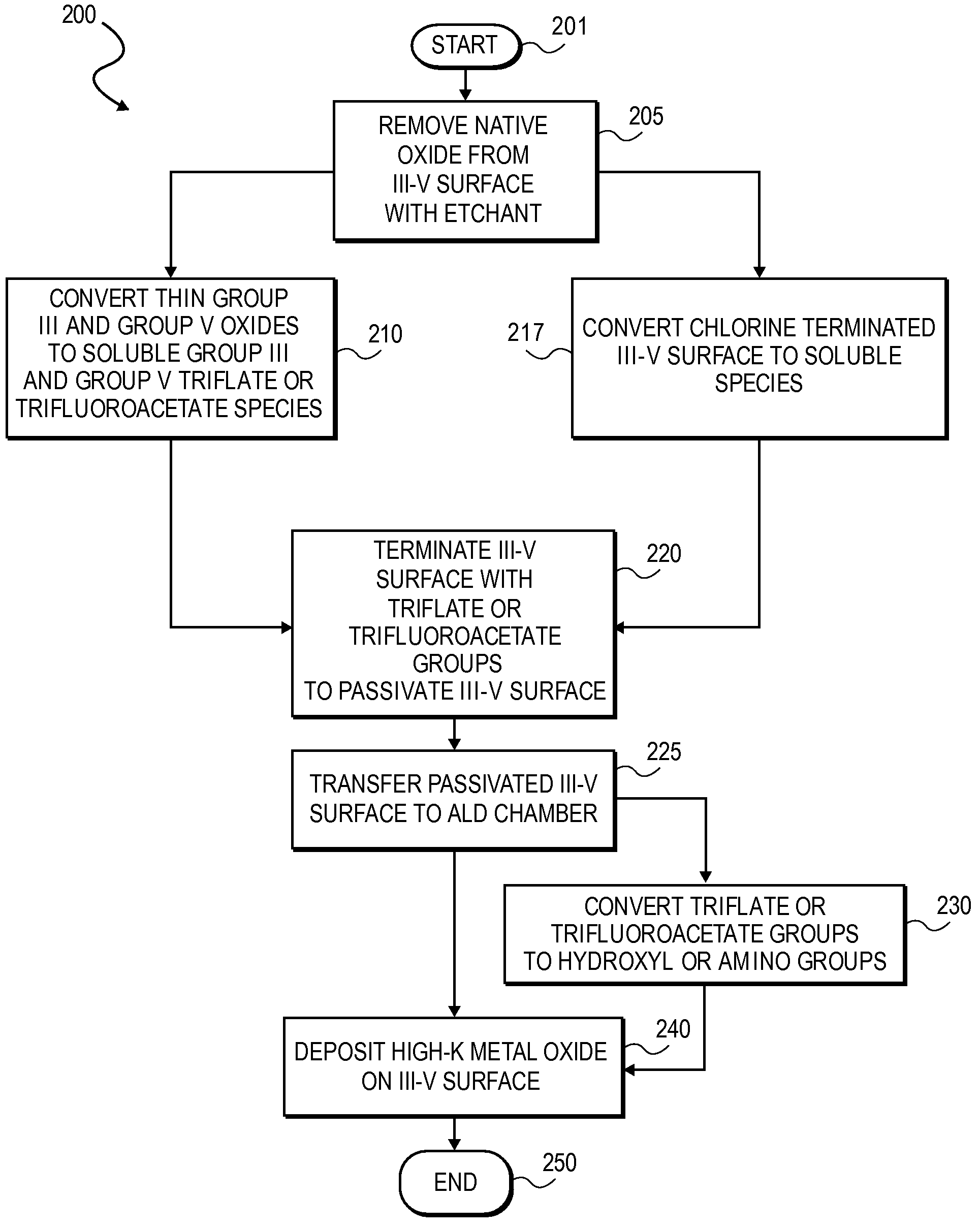
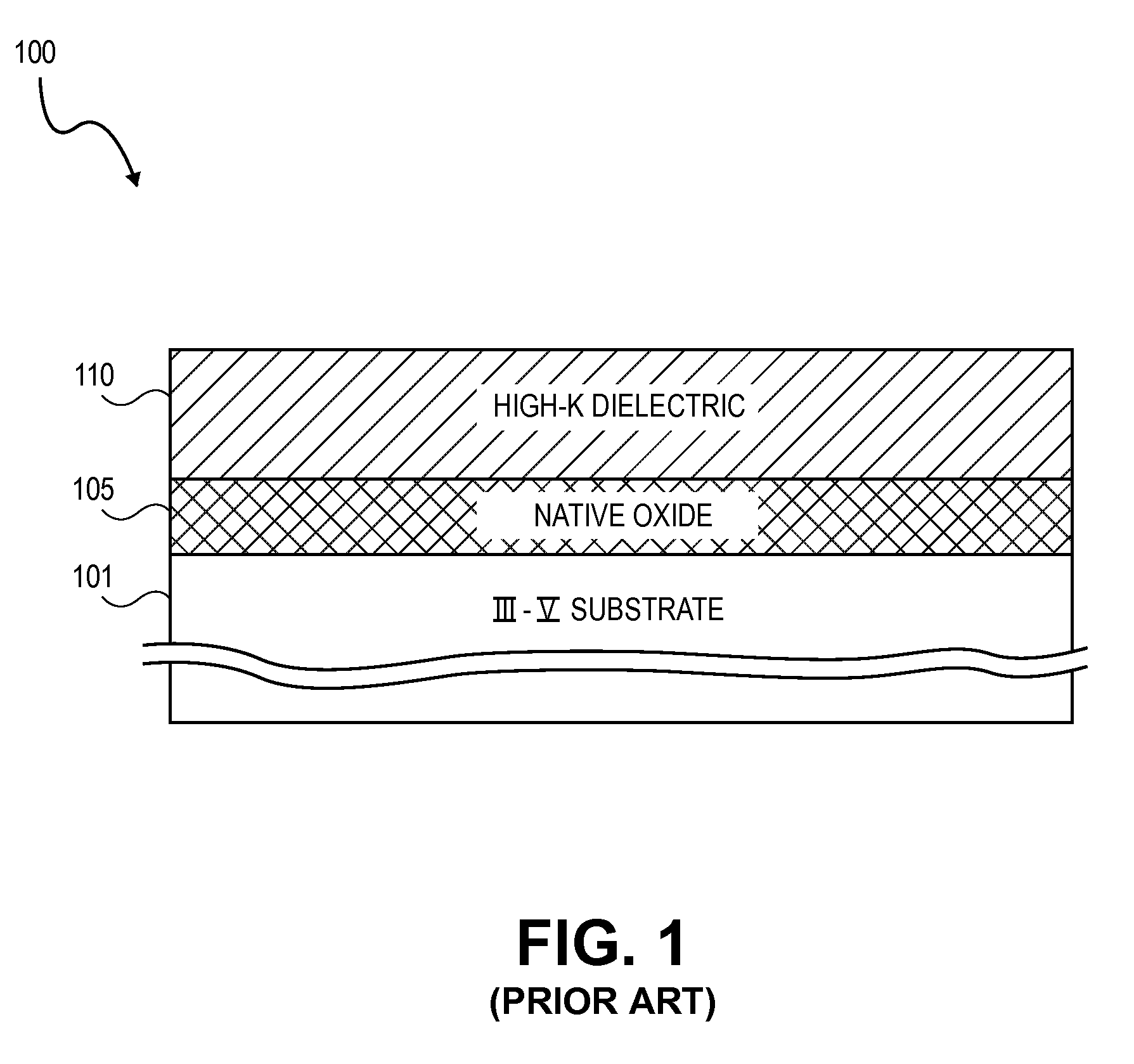
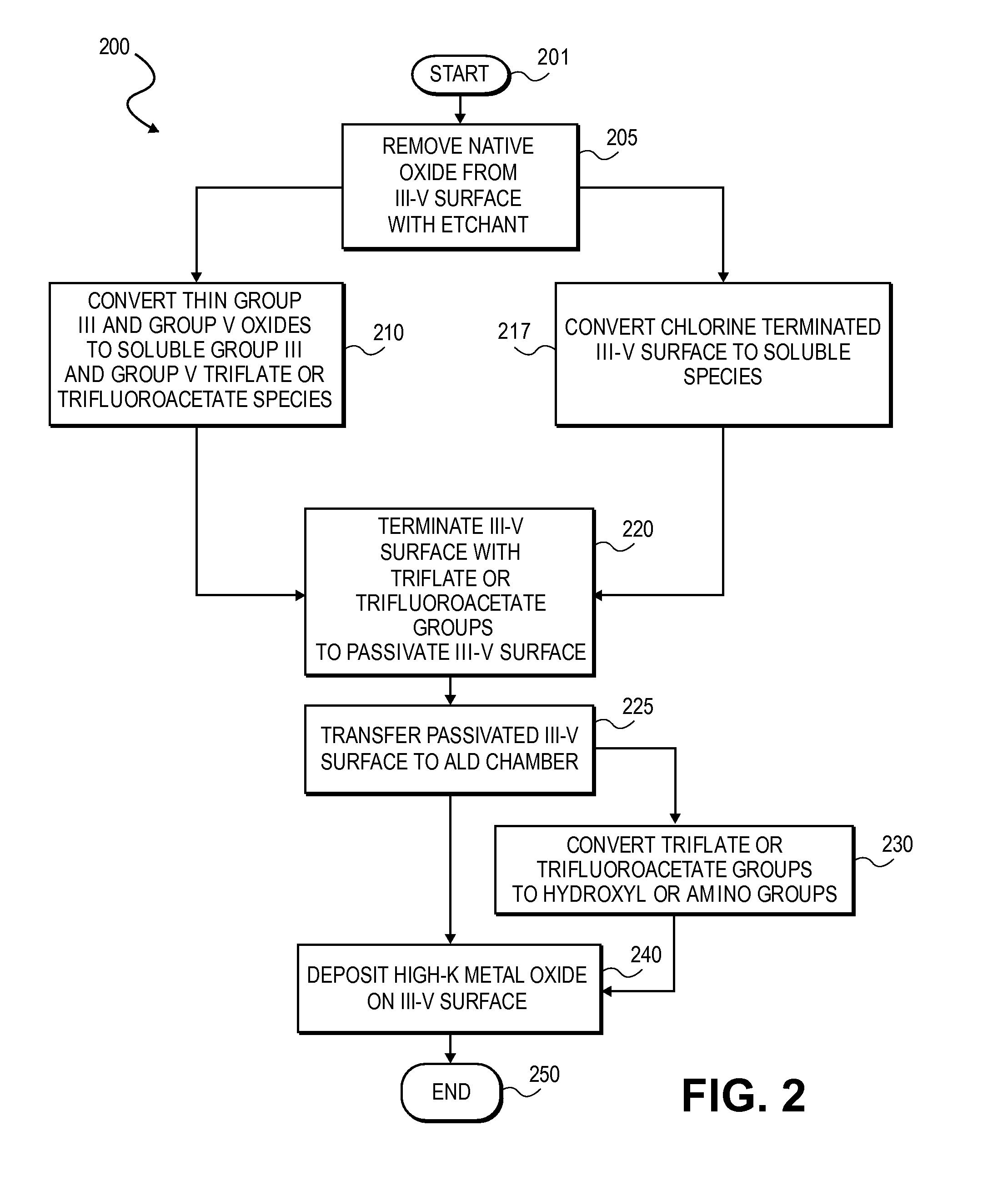
[0016]In various embodiments, surface preparation and ALD film growths on compound semiconductor surfaces are described with reference to figures. However, certain embodiments may be practiced without one or more of these specific details, or in combination with other known methods and materials. In the following description, numerous specific details are set forth, such as specific materials, dimensions and processes, etc., in order to provide a thorough understanding of the present invention. In other instances, well-known semiconductor processes and manufacturing techniques have not been described in particular detail in order to not unnecessarily obscure the present invention. Reference throughout this specification to “an embodiment” means that a particular feature, structure, material, or characteristic described in connection with the embodiment is included in at least one embodiment of the invention. Thus, the appearances of the phrase “in an embodiment” in various places th...


PUM

PropertyMeasurementUnit
temperatureaaaaaaaaaa
binding energyaaaaaaaaaa

Abstract

Surface preparation of a compound semiconductor surface, such as indium antimonide (InSb), with a triflating agent, such as triflic anhydride or a trifluoroacetylating agent, such as trifluoroacetic anhydride is described. In one embodiment, the triflating or trifluoroacetylating passivates the compound semiconductor surface by terminating the surface with triflate trifluoroacetate groups. In a further embodiment, a triflating agent or trifluoroacetylating agent is employed to first convert a thin native oxide present on a compound semiconductor surface to a soluble species. In another embodiment, the passivated compound semiconductor surface is activated in an ALD chamber by reacting the triflate or trifluoroacetate protecting groups with a protic source, such as water (H2O). Metalorganic precursors are then introduced in the ALD chamber to form a good quality interfacial layer, such as aluminum oxide (Al2O3), on the compound semiconductor surface.

Description

BACKGROUND OF THE INVENTION[0001]1. Field of the Invention[0002]The present invention generally relates to the formation of non-native films on surfaces of compound semiconductor films, and more particularly relates to the preparation of III-V semiconductor surfaces for deposition and the subsequent deposition of a film by the Atomic Layer Deposition (ALD) method.[0003]2. Discussion of Related Art[0004]For many decades compound semiconductor materials, such as those formed from alloys of group III atoms with group V atoms (III-V semiconductors), have found limited application in microelectronics primarily because the native oxide which forms on these materials is of very poor quality relative to the native oxide which forms on homogeneous group IV semiconductors, such as silicon (Si). This relatively poor quality of the native oxide degrades the electrical performance of microelectronic devices fabricated from III-V semiconductors. For example, because the native oxide of compound s...

Claims


Application Information

Patent Timeline
Patent Type & Authority Patents(United States)
IPC IPC(8): C23C16/00
CPCH01L21/306H01L21/3141H01L21/0228H01L21/02178
Inventor BLACKWELL, JAMES M.RACHMADY, WILLYKEARNS, GREGORY J.MORRISON, DARRYL J.
Owner INTEL CORP
Why Eureka
Try Eureka