CMOS image sensor and manufacturing method thereof

a technology of metal oxide semiconductor and image sensor, which is applied in the direction of semiconductor devices, electrical equipment, radio control devices, etc., can solve the problems of adverse effects, inability to incorporate a signal processing circuit on the chip of the ccd, and high power consumption, so as to prevent or minimize damage to the photodiode region, improve the characteristics of the image sensor

Active Publication Date: 2010-07-27
DONGBU HITEK CO LTD
View PDF7 Cites 0 Cited by
  • Summary
  • Abstract
  • Description
  • Claims
  • Application Information

AI Technical Summary

Benefits of technology

[0030]An object of the present invention is to provide a CMOS image sensor capable of improving characteristics of the image sensor by preventing or minimizing damage to a photodiode region and a method for manufacturing the same.

Problems solved by technology

The CCD has various disadvantages, such as a complicated driving mode, high power consumption, and inability to incorporate a signal processing circuit on-chip for the CCD due to the many mask processes.
The photodiode region receives light, and is a significantly important region that can be adversely affected by plasma damage during the fabrication process.
In addition, when the interlayer dielectric is selectively removed to form a contact hole, a third plasma damage may be applied to the photodiode region.
The multiple plasma damage applied to the photodiode region functions to generate electrons in a state free of light, thereby weakening the CMOS image sensor.

Method used


Image

  • CMOS image sensor and manufacturing method thereof
  • CMOS image sensor and manufacturing method thereof
  • CMOS image sensor and manufacturing method thereof

Examples


Embodiment Construction

[0043]Reference will now be made in detail to the preferred embodiments of the present invention, examples of which are illustrated in the accompanying drawings. Wherever possible, the same reference numbers will be used throughout the drawings to refer to the same or like parts.

[0044]Hereinafter, a CMOS image sensor and a method for manufacturing the same according to an embodiment of the present invention will be explained with reference to the accompanying drawings.

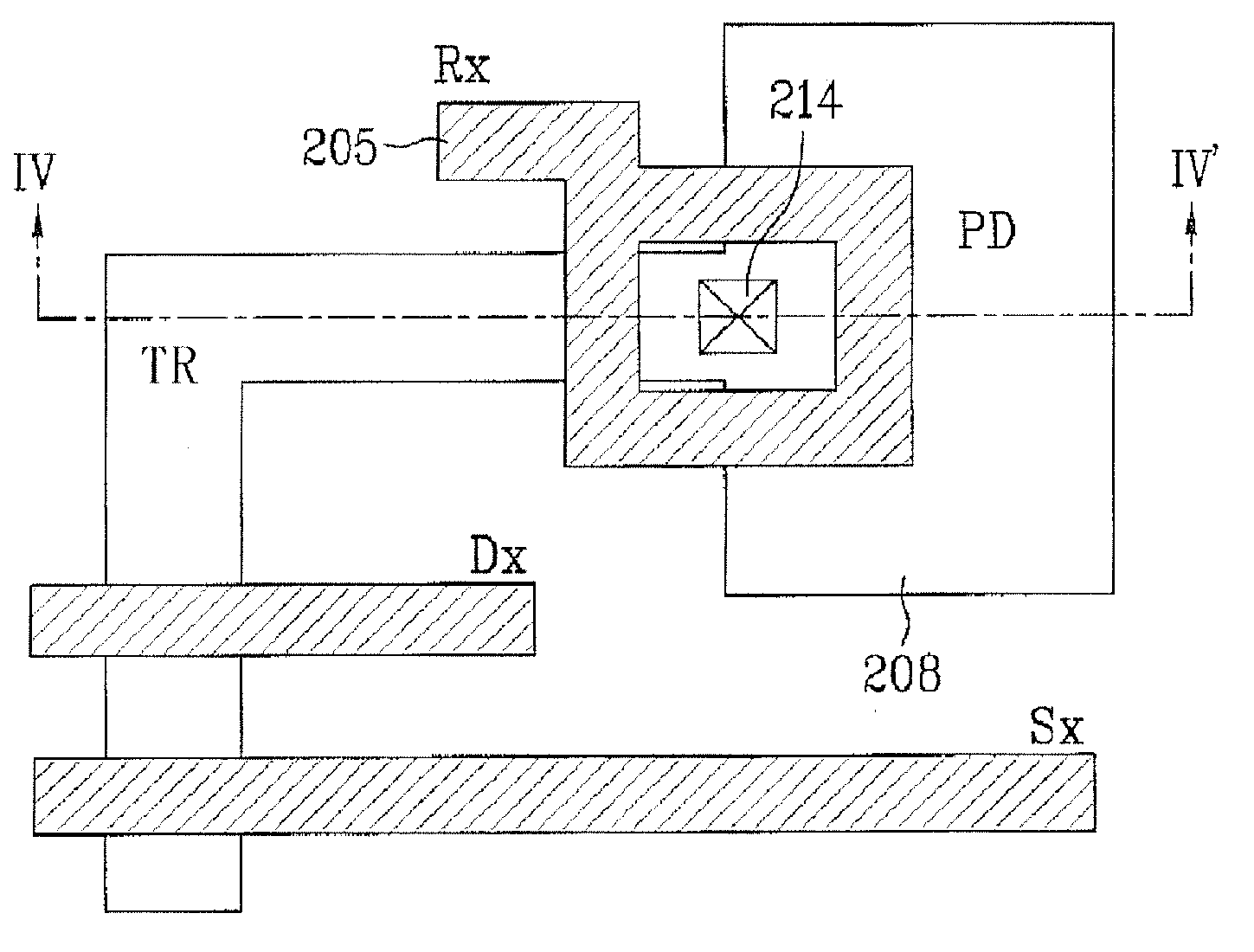
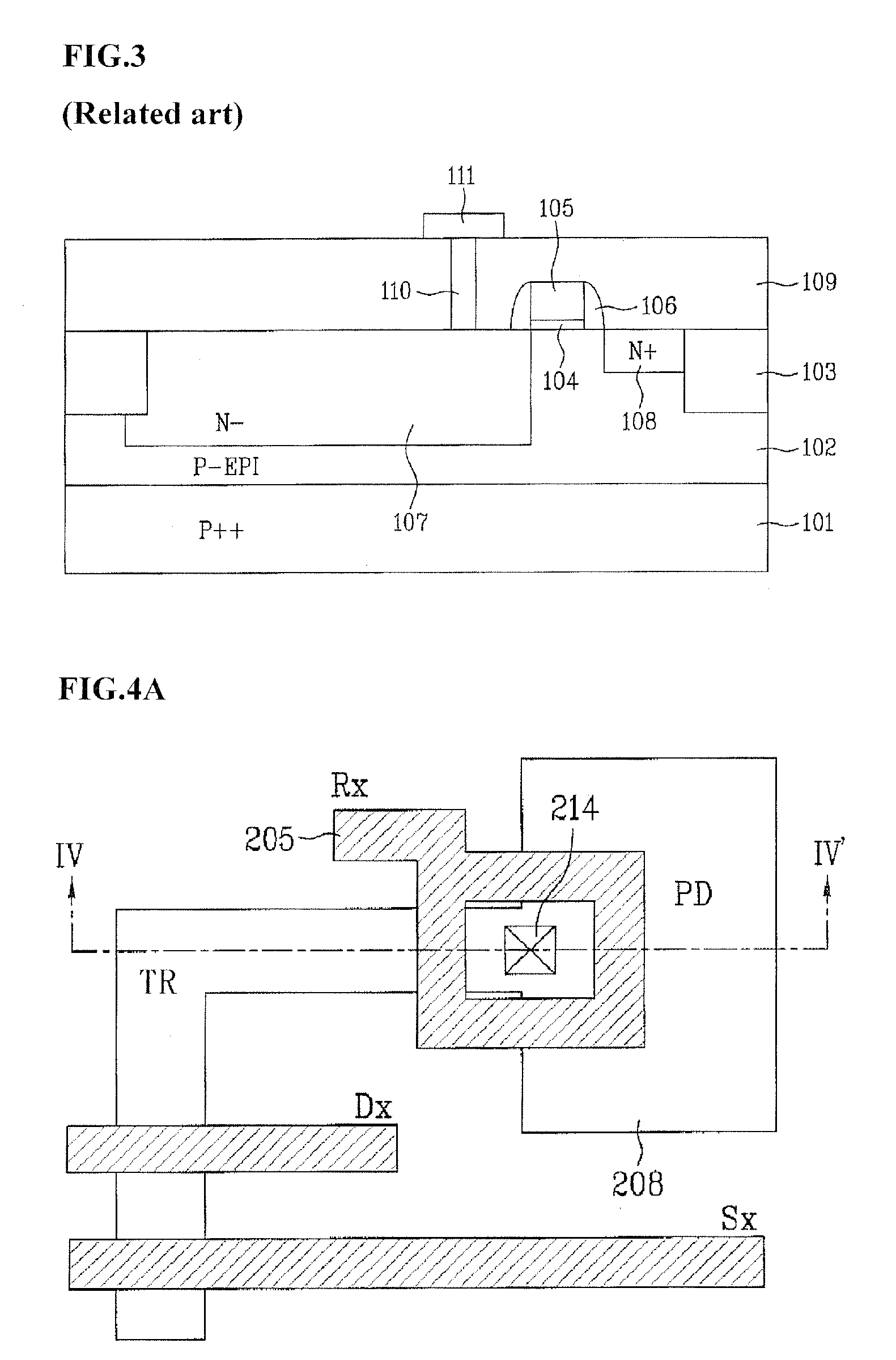
[0045]FIG. 4A is a layout view showing a unit pixel of a CMOS image sensor according to an embodiment of the present invention. FIG. 4B is a cross-sectional view of the CMOS image sensor of FIG. 4 taken along the line IV-IV′.

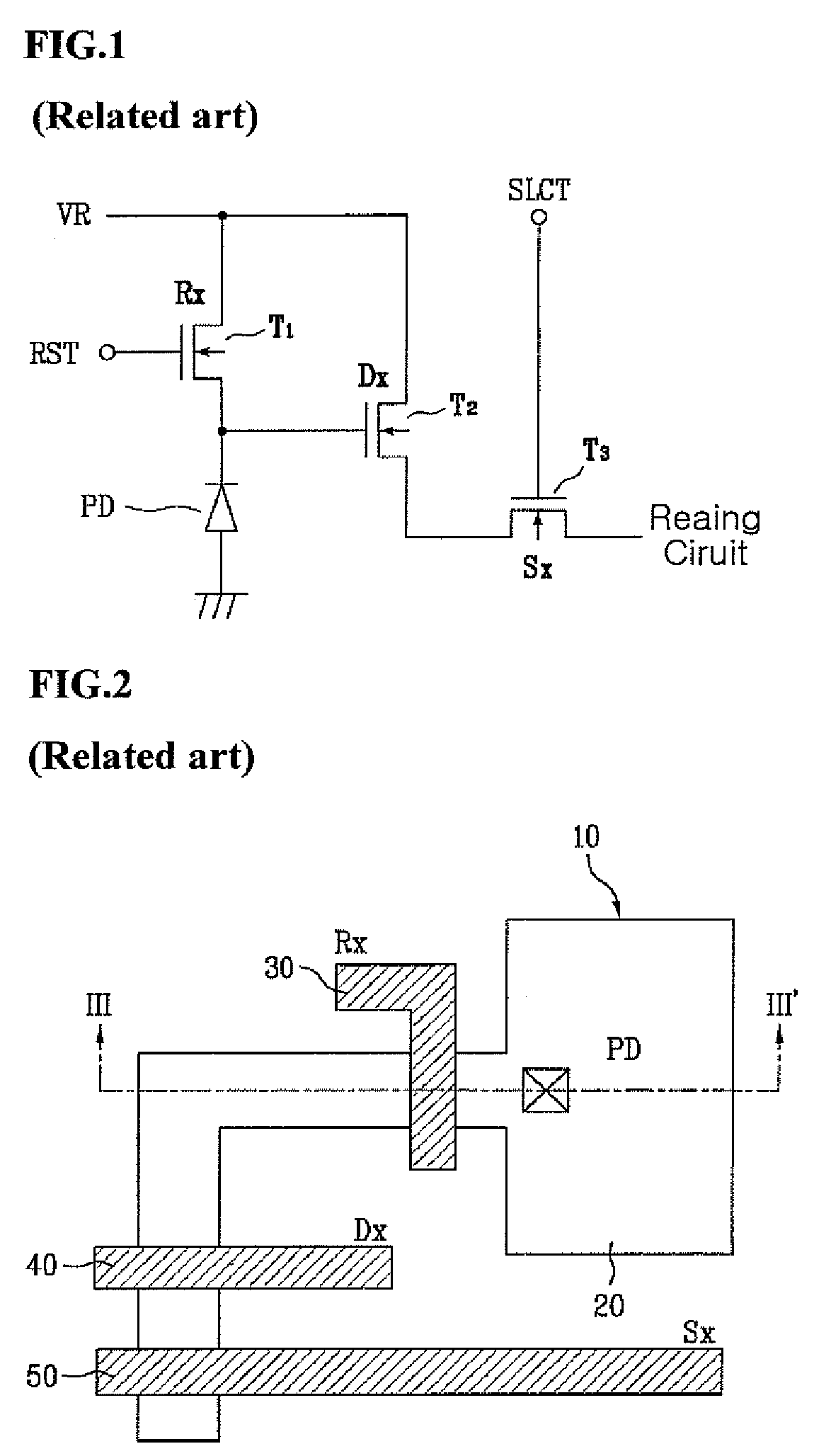
[0046]Referring to FIG. 4A and FIG. 4B, a CMOS image sensor can include a semiconductor substrate 201 having a device isolation region and an active region defined therein. The active region includes a photodiode region PD and a transistor region TR.

[0047]A device isolation layer 203 can be formed ...


PUM


Abstract

A CMOS image sensor capable of improving characteristics of the image sensor by preventing damage to a photodiode region and a method for manufacturing the same are provided. The CMOS image sensor includes: a semiconductor substrate on which a device isolation region and an active region are defined; a photodiode region formed at the active region; a conductive plug formed on the photodiode region for connecting the photodiode region to a metal wiring; and a transistor formed enclosing the conductive plug.

Description

RELATED APPLICATION[0001]This application claims the benefit under 35 U.S.C. §119(e), of Korean Patent Application Number 10-2005-0132650 filed Dec. 28, 2005, which is incorporated herein by reference in its entirety.FIELD OF THE INVENTION[0002]The present invention relates to a complementary metal oxide semiconductor (CMOS) image sensor and a method for manufacturing the same.BACKGROUND OF THE INVENTION[0003]In general, an image sensor is a semiconductor device that transforms an optical image to electrical signals. The image sensor is generally classified as a charge coupled device (CCD) or a CMOS image sensor.[0004]The CCD type image sensor includes several MOS (metal oxide semiconductor) capacitors, closely positioned to one another, in which electric charge carriers are transferred to or saved in the MOS capacitors.[0005]The CMOS image sensor has incorporated a switching mode by forming MOS transistors for each unit pixel with CMOS technology and using control circuits and sign...

Claims


Application Information

Patent Timeline
Patent Type & Authority Patents(United States)
IPC IPC(8): H01L31/062H01L31/113
CPCH01L27/14603H01L27/1463H01L27/146
Inventor HAN, CHANG HUN
Owner DONGBU HITEK CO LTD
Why Eureka
Try Eureka