Method for mechanical packaging of electronics

a mechanical packaging and electronics technology, applied in the direction of casings/cabinets/drawers, electrical apparatus construction details, casings/cabinets/drawers details, etc., can solve the problems of inferior electrical conductivity, high cost of thick film conductor production, and easy fracture of substrates, etc., to achieve improved electronic performance, cost effective

Active Publication Date: 2010-08-03
SYNQOR
View PDF7 Cites 20 Cited by
  • Summary
  • Abstract
  • Description
  • Claims
  • Application Information

AI Technical Summary

Benefits of technology

[0005]There is a need for cost effective mechanical packaging for Hi-Rel converters and filter modules which enable advances in electronic performance while maintaining physical integrity and reducing product weight. The advent of suitable plastic packaged electronic components now permits their use in products that were typically produced in hermetically sealed enclosures. These plastic device packages provide sufficient protection for the active microcircuits contained within so that the exterior mechanical packaging itself is no longer required to be hermetically sealed.
[0006]The mechanical packaging is considered to be the enclosure that protects the electronic components from the diverse environmental stresses to be encountered such as, but not limited to, thermal extremes, mechanical shock and vibration, adverse chemical or sand exposures, etc. This packaging should be robust in order to provide the desired protection, but also be easy to produce and assemble in order to be cost effective.

Problems solved by technology

The substrates are prone to fracture during fabrication, mounting of electronic components, base plate attachment and use in the field.
The thick film conductors are expensive to produce and have inferior electrical conductivity compared to pure metals and can only be fabricated in limited thicknesses, resulting in relatively high electrical resistances which reduce the efficiency.
Interconnection between components is limited because of the low layer count and limitations on the use of vertical integration access (vias).
Handling and assembly of the bare silicon microcircuits requires the use of expensive clean room environments and specialized handling and even dress of assembly personnel.
The wire bonds that connect the microcircuits to the substrate are prone to fatigue or tensile failures under extreme vibration or acceleration conditions.
The use of Molybdenum and KOVAR result in a heavy package.
All of the material systems as described above require assembly processes that are not conducive to low cost, high volume manufacturing.
Furthermore, the final assembly has a limited ability to withstand shock and vibration stresses encountered under service conditions.

Method used


Image

  • Method for mechanical packaging of electronics
  • Method for mechanical packaging of electronics
  • Method for mechanical packaging of electronics

Examples


Embodiment Construction

[0014]A description of preferred embodiments of the invention follows.

[0015]New methods for the design of a Hi-Rel mechanical package and the subsequent assembly of the circuit within it have been developed. The methods provide lower cost and are easier to produce using standard, high volume production methods and equipment.

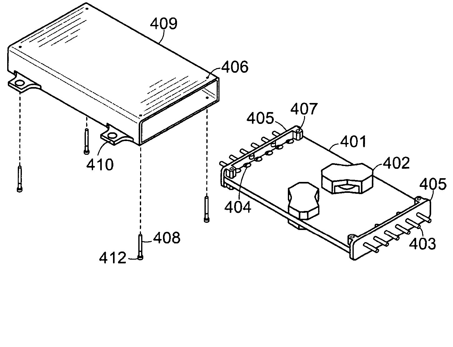
[0016]FIG. 4 shows an exploded view of one embodiment of the new construction / assembly. The basic principles of this method are as follows.

[0017]The substrate is made from a printed circuit board 401 (PCB) fabricated from layers of fiberglass and copper foil. PCB assemblies are inherently more mechanically robust than ceramic substrate assemblies. The PCB enables the use of pure metal, multiple layers (8-12 typical), and metal thicknesses up to 6 times those of typical thick film conductions. The conductor layers are made from copper foil, and provide higher conductivity resulting in significantly lower interconnection resistance and a resulting increase in effic...


PUM

PropertyMeasurementUnit
thermally conductiveaaaaaaaaaa
thermal conductionaaaaaaaaaa
electrical isolationaaaaaaaaaa

Abstract

Electronics mounted on a printed circuit board are housed within a high conductivity case with connecting pins extending therethrough. The case is filled with thermally conductive potting material to provide thermal conduction from the printed circuit board to the case. The case may be a conduit having open ends through which the printed circuit board is inserted or it may comprise a cover mounted to a base plate.

Description

RELATED APPLICATION[0001]This application claims the benefit of U.S. Provisional Application No. 60 / 707,605, filed on Aug. 11, 2005. The entire teachings of the above application are incorporated herein by reference.BACKGROUND OF THE INVENTION[0002]There are standard package designs for certain types of military grade DC-DC converters, filters and other electronic circuits such as those shown in FIGS. 1 and 2. The typical prior art for constructing these circuits and assembling them in their packages is shown in FIG. 3. A ring frame 301 (typically KOVAR) is welded to a base plate 302 (typically Molybdenum). A ceramic substrate 303 (typically Alumina, Aluminum Nitride, or Beryllium Oxide) is bonded to the base plate using epoxies or solder alloys if the substrate is suitably plated. Electronic components are soldered to the substrate which also contains thick and or thin film conductors. Most of the active microcircuits 304 (e.g. MOSFETs, diodes, control IC's) are soldered or epoxied...

Claims


Application Information

Patent Timeline
Patent Type & Authority Patents(United States)
IPC IPC(8): H05K7/14H05K7/20H05K13/00
CPCH05K7/1417H05K7/20463Y10T29/49146Y10T29/49176Y10T29/49171
Inventor PITZELE, LENNARTDANCY, ABRAM P.LAWHITE, LEIF E.HEMOND, RENESCHLECHT, MARTIN F.
Owner SYNQOR
Why Eureka
Try Eureka