Supercharge Your Innovation With Domain-Expert AI Agents!

Imaging post structures using x and y dipole optics and a single mask

a dipole optic and post structure technology, applied in the field of photolithographic techniques, can solve problems such as new challenges

Inactive Publication Date: 2010-09-14
SANDISK TECH LLC
View PDF14 Cites 6 Cited by
  • Summary
  • Abstract
  • Description
  • Claims
  • Application Information

AI Technical Summary

Benefits of technology

This method effectively achieves improved resolution and feature size reduction, allowing for the formation of precise patterns and structures like post structures or voids in integrated circuits, enhancing the capabilities of photolithography in fabricating smaller integrated circuit components.

Problems solved by technology

While photolithography is a relatively mature technology, new challenges are encountered by the ever present desire to scale down feature sizes.

Method used


Image

  • Imaging post structures using x and y dipole optics and a single mask
  • Imaging post structures using x and y dipole optics and a single mask
  • Imaging post structures using x and y dipole optics and a single mask

Examples


Embodiment Construction

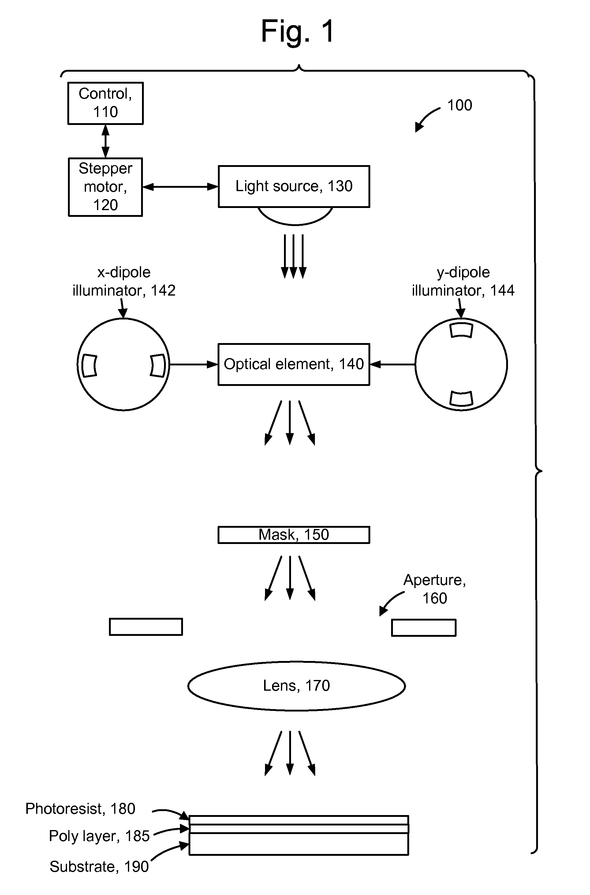
[0039]The present invention provides a photolithographic method for fabricating a pattern on a substrate using different exposure patterns.

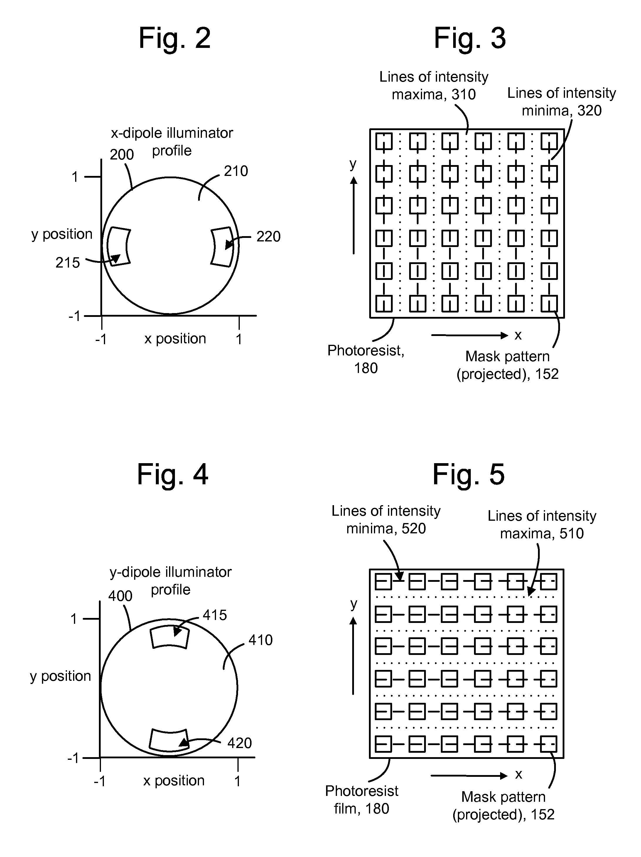
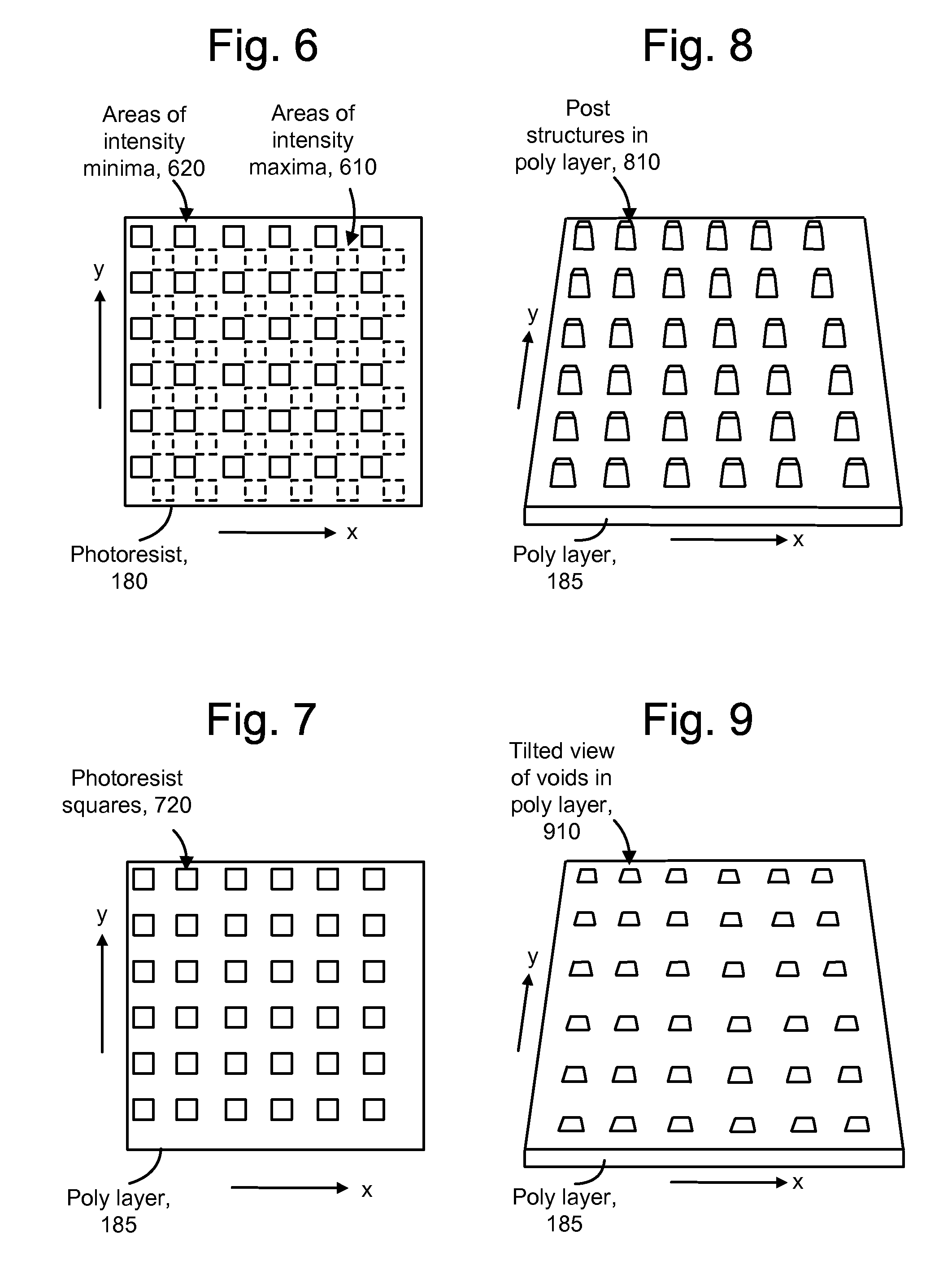
[0040]FIG. 1 depicts a photolithographic apparatus. The apparatus, shown generally at 100, includes a control 110, stepper motor 120, light source 130, optical element 140, mask 150, aperture 160 and projection lens 170. A pattern of the mask 150 is transferred to a photoresist film 180 on a substrate 190 such as a wafer. A polysilicon (poly) layer 185 is provided on the substrate in an example implementation. Other materials can be used instead of poly in a layer beneath the photoresist film 180, such as tungsten or other metal substrate. The photoresist film has a pre-determined thickness which is suitable for its intended application. In this simplified example, under control of the stepper motor 120, the light source 130 and optical element 140 move relative to the mask 150, while the photoresist film 180 is held in a fixed position in relati...


PUM

PropertyMeasurementUnit
wavelengthaaaaaaaaaa
feature sizeaaaaaaaaaa

Abstract

A photolithographic method uses different exposure patterns. In one aspect, a photo-sensitive layer on a substrate is subject to a first exposure using optics having a first exposure pattern, such as an x-dipole pattern, followed by exposure using optics having a second exposure pattern, such as a y-dipole pattern, via the same mask, and with the photo-sensitive layer fixed relative to the mask. A 2-D post pattern with a pitch of approximately 70-150 nm may be formed in a layer beneath the photo-sensitive layer using 157-193 nm UV light, and hyper-numerical aperture optics, in one approach. In another aspect, hard baking is performed after both of the first and second exposures to erase a memory effect of photoresist after the first exposure. In another aspect, etching of a hard mask beneath the photo-sensitive layer is performed after both of the first and second exposures.

Description

BACKGROUND OF THE INVENTION[0001]1. Field of the Invention[0002]The present invention relates to photolithographic techniques for use in fabricating integrated circuits.[0003]2. Description of the Related Art[0004]Photolithography is a photographic process used to transfer circuit patterns onto a semiconductor wafer. The process generally involves projecting light through a patterned mask onto a silicon wafer which is covered with a photosensitive film, e.g., photoresist. A stepper move across the mask, projecting light through the mask to image portions of the photoresist corresponding to the mask pattern. The wafer is then developed so that the exposed or unexposed portions of the photoresist are removed, depending on the type of resist used. While photolithography is a relatively mature technology, new challenges are encountered by the ever present desire to scale down feature sizes.SUMMARY OF THE INVENTION[0005]The present invention addresses the above and other issues by provid...

Claims


Application Information

Patent Timeline
Patent Type & Authority Patents(United States)
IPC IPC(8): G03F7/20
CPCG03F1/00G03F7/70425G03F7/70466
Inventor CHEN, YUNG-TINRADIGAN, STEVEN J.POON, PAULKONEVECKI, MICHAEL W.
Owner SANDISK TECH LLC
Features
  • R&D
  • Intellectual Property
  • Life Sciences
  • Materials
  • Tech Scout
  • Unparalleled Data Quality
  • Higher Quality Content
  • 60% Fewer Hallucinations
Learn More