Method for removing damaged dielectric material

a dielectric film and removal process technology, applied in the field of dielectric film removal, can solve the problems of affecting the quality of dielectric films

Inactive Publication Date: 2010-09-14
TOKYO ELECTRON LTD
View PDF23 Cites 45 Cited by
  • Summary
  • Abstract
  • Description
  • Claims
  • Application Information

AI Technical Summary

Benefits of technology

[0062]Although only certain exemplary embodiments of inventions have been described in detail above, those skilled in the art will readily appreciate that many modifications are possible in the exemplary embodiments without materially departing from the novel teachings and advantages of this invention.

Problems solved by technology

As is known to those in the semiconductor art, interconnect delay is a major limiting factor in the drive to improve the speed and performance of integrated circuits (IC).
While low-k materials are promising for fabrication of semiconductor circuits, the present inventors have recognized that these films also provide many challenges.
First, low-k films tend to be less robust than more traditional dielectric layers and can be damaged during wafer processing, such as by etch and plasma ashing processes generally used in patterning the dielectric layer.
Further, some low-k films tend to be highly reactive when damaged, particularly after patterning, thereby allowing the low-k material to absorb water and / or react with other vapors and / or process contaminants that can alter the electrical properties of the dielectric layer.

Method used


Image

  • Method for removing damaged dielectric material
  • Method for removing damaged dielectric material
  • Method for removing damaged dielectric material

Examples


Embodiment Construction

[0017]In the following description, in order to facilitate a thorough understanding of the invention and for purposes of explanation and not limitation, specific details are set forth, such as a particular geometry of the treatment system and descriptions of various components and processes used therein. However, it should be understood that the invention may be practiced in other embodiments that depart from these specific details.

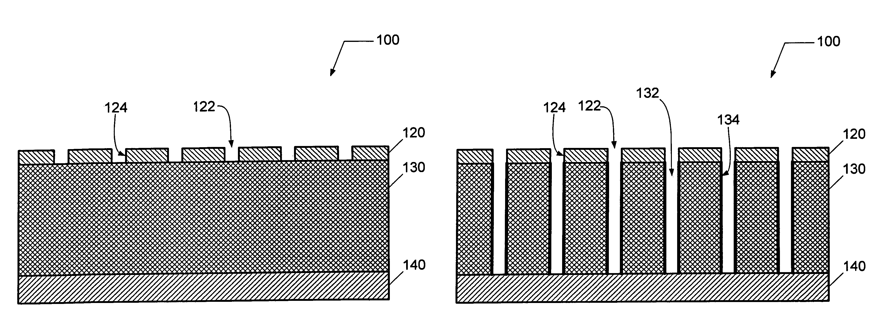
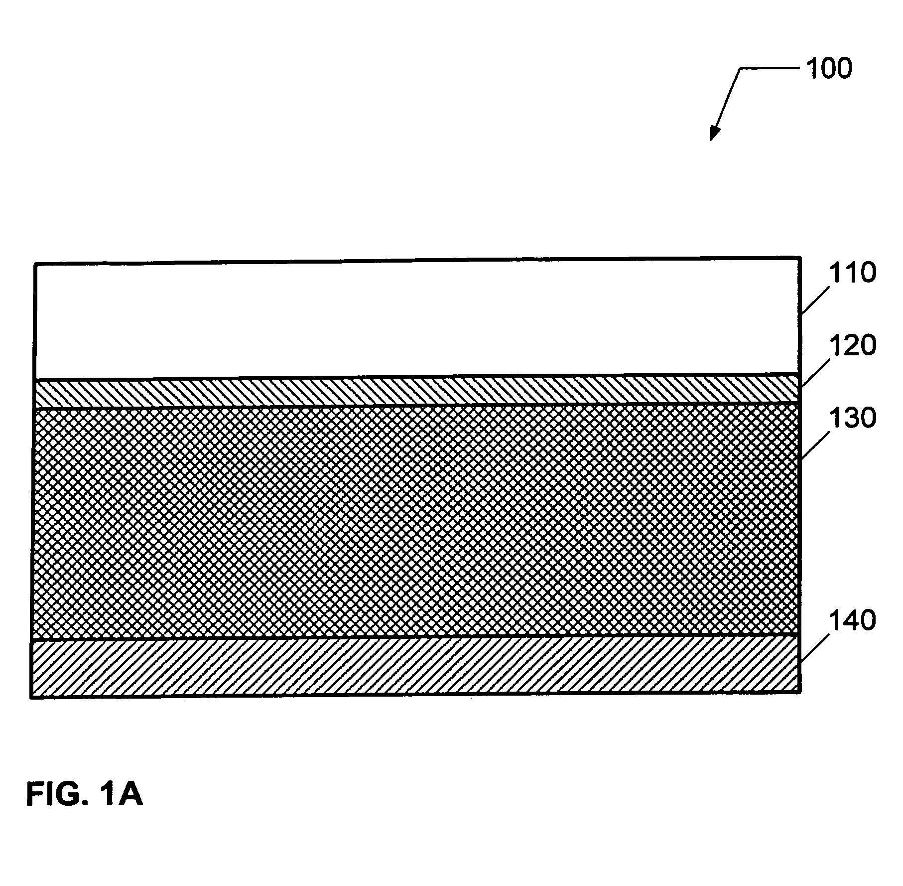
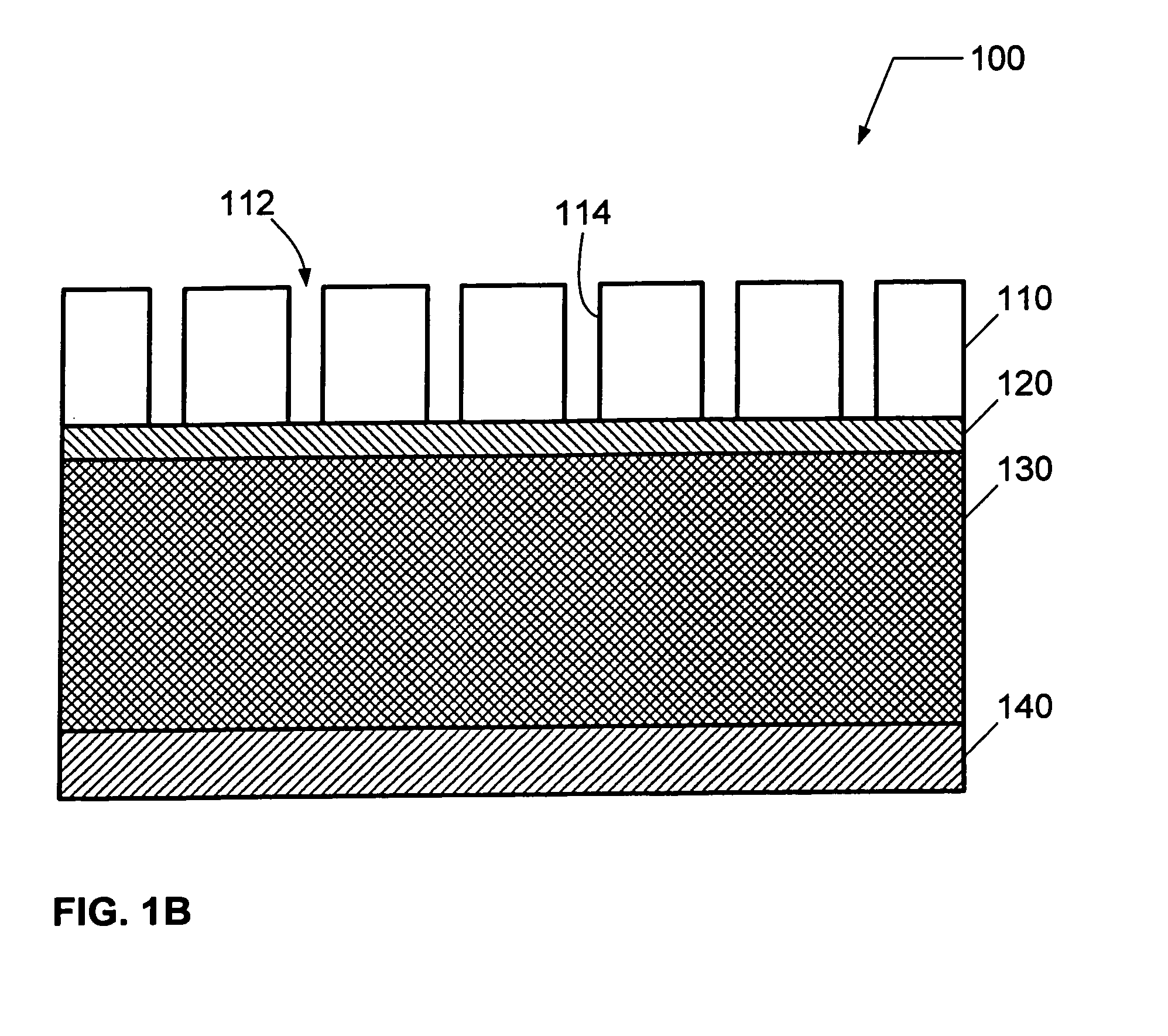
[0018]In material processing methodologies, pattern etching comprises the application of a thin layer of light-sensitive material, such as photoresist, to an upper surface of a substrate, that is subsequently patterned in order to provide a mask for transferring this pattern to the underlying thin film during etching. The patterning of the light-sensitive material generally involves exposure by a radiation source through a reticle (and associated optics) of the light-sensitive material using, for example, a photo-lithography system, followed by the remova...


PUM

PropertyMeasurementUnit
dielectric constantaaaaaaaaaa
pressureaaaaaaaaaa
dielectric constantaaaaaaaaaa

Abstract

A method for removing a damaged dielectric material following an etch process, an ashing process, or a wet cleaning process is described. A dry, non-plasma removal process is implemented to remove a thin layer of damaged material on a feature following formation of the feature. The dry, non-plasma removal process includes a chemical treatment of the damaged material, followed by a thermal treatment of the chemically treated surface layer. The two steps, chemical and thermal treatment, can be repeated.

Description

BACKGROUND OF THE INVENTION[0001]1. Field of Invention[0002]The present invention relates to a method for performing a removal process on a dielectric film, and more particularly to a method for removing damaged layers on a low dielectric constant (low-k) film following an etching or ashing process.[0003]2. Description of Related Art[0004]As is known to those in the semiconductor art, interconnect delay is a major limiting factor in the drive to improve the speed and performance of integrated circuits (IC). One way to minimize interconnect delay is to reduce interconnect capacitance by using low dielectric constant (low-k) materials during production of the IC. Such low-k materials have also proven useful for low temperature processing. Thus, in recent years, low-k materials have been developed to replace relatively high dielectric constant insulating materials, such as silicon dioxide. In particular, low-k films are being utilized for inter-level and intra-level dielectric layers b...

Claims


Application Information

Patent Timeline
Patent Type & Authority Patents(United States)
IPC IPC(8): H01L21/302
CPCH01L21/02063H01L21/31116H01L21/76814H01L21/76802H01L21/31138C03C15/00C03C25/68
Inventor BROWN, IAN J.
Owner TOKYO ELECTRON LTD
Why Eureka
Try Eureka