Two step process for uniform across wafer deposition and void free filling on ruthenium coated wafers

a ruthenium coating and ruthenium seed technology, applied in the direction of electrolysis process, semiconductor devices, electrolysis components, etc., can solve the problems of difficult or impossible filling of features with electroplating process, less conformal film covering trench sidewalls and bottoms, and high cost of cvd methods compared to pvd processes. achieve the effect of reducing the resistivity of the very thin film deposited and enhancing the nucleation density

Active Publication Date: 2010-09-21
NOVELLUS SYSTEMS
View PDF75 Cites 32 Cited by
  • Summary
  • Abstract
  • Description
  • Claims
  • Application Information

AI Technical Summary

Benefits of technology

[0006]The present invention addresses these needs by providing a two-step semiconductor electroplating process that deposits copper onto wafers coated with a semi-noble metal in uniform and void-free manner. The semi-noble metal is sufficiently conductive to allow direct electroplating of a copper seed layer. It may also serve as all or a portion of the diffusion barrier used in Damascene processing. Electroplating in an appropriate plating bath nucleates copper uniformly and conformably at a high density in a very thin film. The resulting copper seed layer is thinner and more conformal than those produced using traditional PVD copper seed processes. A unique pulsed waveform may be employed to enhance the nucleation density and reduces resistivity of the very thin film deposited in the nucleation operation. After the copper seed layer is formed, electroplating in a different electrolyte fills the features.

Problems solved by technology

Chemical vapor deposition (CVD) methods can deposit a conformal copper seed layer with good adhesion, but CVD methods are expensive as compared to PVD processes.
Physical vapor deposition (PVD) methods can deposit a copper seed layer with good adhesion, but produces a less conformal film that covers the sidewalls and bottoms of trenches poorly.
The thicker PVD seed layer increases aspect ratios in features and may pinch off the gap opening, making the features harder or impossible to fill with an electroplating process.
As feature sizes decrease, the limitation of a PVD seed layer restricts how small metal lines can be.

Method used


Image

  • Two step process for uniform across wafer deposition and void free filling on ruthenium coated wafers
  • Two step process for uniform across wafer deposition and void free filling on ruthenium coated wafers
  • Two step process for uniform across wafer deposition and void free filling on ruthenium coated wafers

Examples


examples

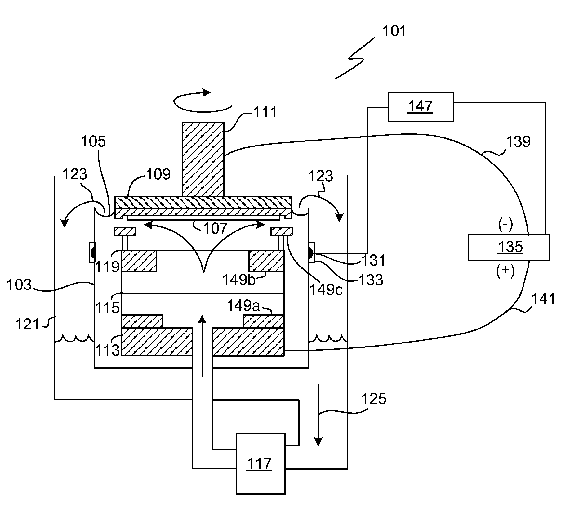
[0067]Copper seed layers were electroplated onto ruthenium coated 300 mm blanket wafers in accordance with the present invention. The ruthenium thickness was 30 angstroms. The seed layer electrolyte used comprises 0.005M copper nitrate, 0.0055M EDTA, and DI water. DI water was replaced as it evaporates to keep the bath conductivity constant at about 0.9 milliSiemens. The electrolyte pH was about 3.7.

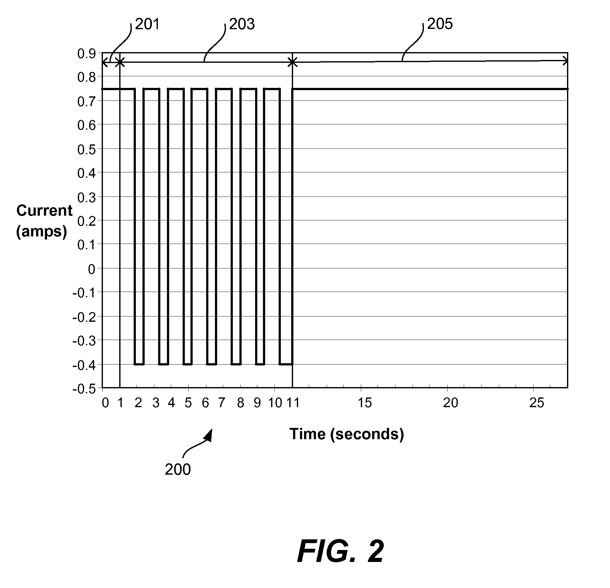
[0068]FIG. 5 shows the thickness measurements at various points on three wafers, each deposited to a different thickness. The x-axis shows the thickness in angstroms measured at various y-axis wafer positions. Each wafer was deposited using a current waveform having three steps. The first step is a direct current of 0.75 amps for 1 second. The second step is alternating pulses of forward current at 0.75 amps for 900 milliseconds and reverse current at 0.4 amps for 500 milliseconds for a total second step duration of 10 seconds. The third step is a direct current of 0.75 amps. The duratio...


PUM

PropertyMeasurementUnit
resistivityaaaaaaaaaa
temperatureaaaaaaaaaa

Abstract

A two-step semiconductor electroplating process deposits copper onto wafers coated with a semi-noble metal in manner that is uniform across the wafer and free of voids. A plating bath nucleates copper uniformly and conformably at a high density in a very thin film. A second bath fills the features. A unique pulsed waveform enhances the nucleation density and reduces resistivity of the very thin film deposited in the nucleation operation. The process produces a thinner and conformal copper seed film than traditional PVD copper seed processes.

Description

FIELD OF THE INVENTION[0001]The present invention relates generally to methods and apparatus for depositing copper onto a wafer and more particularly to methods and apparatus for electroplating a copper seed layer on a semiconductor wafer. It is particularly useful for electroplating copper in damascene and dual damascene integrated circuit fabrication methods.BACKGROUND OF THE INVENTION[0002]Manufacturing of semiconductor devices commonly requires deposition of electrically conductive material on semiconductor wafers. The conductive material, such as copper, is often deposited by electroplating onto a seed layer of copper deposited onto the wafer surface by a PVD or CVD method. Electroplating is a method of choice for depositing metal into the vias and trenches of the processed wafer during damascene and dual damascene processing.[0003]Damascene processing is used for forming interconnections on integrated circuits (ICs). Damascene processing involves formation of inlaid metal line...

Claims


Application Information

Patent Timeline
Patent Type & Authority Patents(United States)
IPC IPC(8): H01L21/44
CPCC25D3/38C25D5/02C25D5/10C25D5/18H01L21/76864H01L21/76873C25D7/123H01L21/2885C25D17/001H01L21/76877C25D5/619
Inventor REID, JONATHANPARK, SEYANGVARADARAJAN, SESHASAYEEDOUBINA, NATALIA
Owner NOVELLUS SYSTEMS
Why Eureka
Try Eureka