High-mobility n-type ultrathin nano diamond film and preparation method thereof

A nano-diamond and high-mobility technology, applied in the field of high-mobility n-type ultra-thin nano-diamond film and its preparation, can solve problems such as poor electrical conductivity and affect the electrical performance of the film, and achieves a simple method, improved electrical performance, and easy operation. Effect

Active Publication Date: 2018-09-14
ZHEJIANG UNIV OF TECH
View PDF7 Cites 7 Cited by
  • Summary
  • Abstract
  • Description
  • Claims
  • Application Information

AI Technical Summary

Problems solved by technology

At the same time, the conductivity of the amorphous carbon grain boundary in the nanodiamond film is poor, which also affects the electrical properties of the film.

Method used


Image

  • High-mobility n-type ultrathin nano diamond film and preparation method thereof
  • High-mobility n-type ultrathin nano diamond film and preparation method thereof
  • High-mobility n-type ultrathin nano diamond film and preparation method thereof

Examples


Embodiment 1

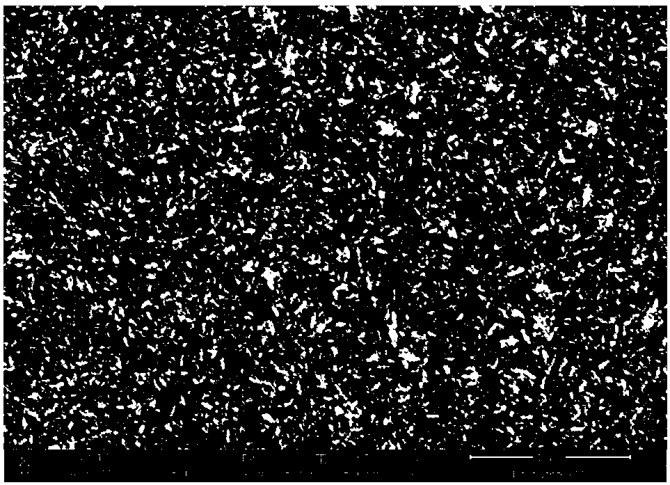
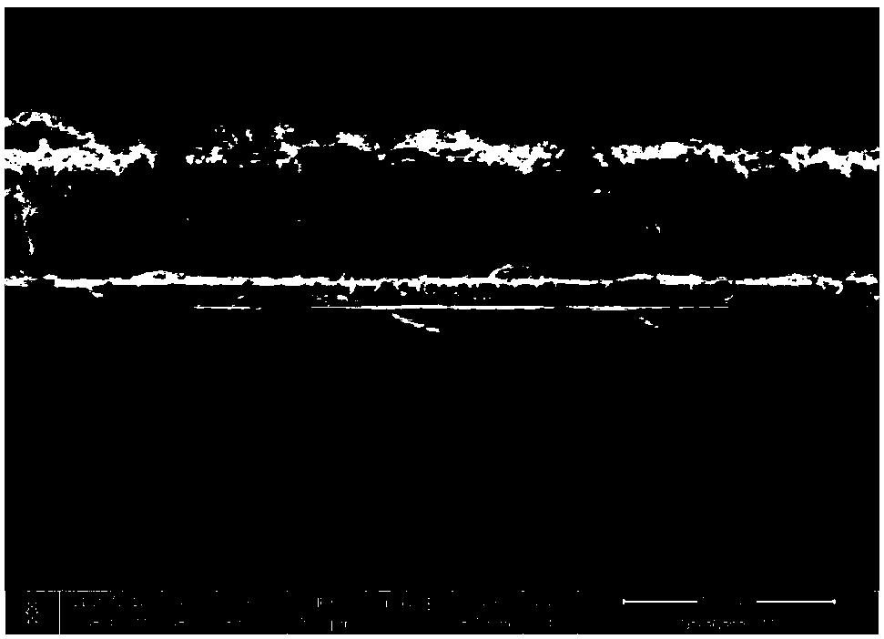
[0028]The high-resistance silicon wafer was cleaned twice with acetone and dried as the substrate for depositing the AlN transition layer. The silicon wafer was placed on the reaction turntable of SPC-350 multi-target magnetron sputtering apparatus, with high-purity aluminum target as the target material, the reaction power was 100W, and the reaction pressure was 0.8KPa. The nitrogen flow rate is controlled at 17sccm and the argon flow rate is 5sccm through the flowmeter, and nitrogen and argon are introduced into the vacuum chamber, and the air pressure in the vacuum chamber is adjusted to the working pressure by turning the valve of the molecular pump, and the DC sputtering is turned on Slowly increase the power of the power supply, and after the Al target glows successfully, adjust the sputtering power to the required power and start sputtering. The sputtering time is 15 minutes, and the thickness of the AlN transition layer obtained is about 70 nm. The AlN-deposited high-...

Embodiment 2

[0037] The high-resistance silicon wafer was cleaned twice with acetone and dried as the substrate for depositing the AlN transition layer. The silicon wafer was placed on the reaction turntable of SPC-350 multi-target magnetron sputtering apparatus, with high-purity aluminum target as the target material, the reaction power was 100W, and the reaction pressure was 0.8KPa. The nitrogen flow rate is controlled at 17sccm and the argon flow rate is 5sccm through the flowmeter, and nitrogen and argon are introduced into the vacuum chamber, and the air pressure in the vacuum chamber is adjusted to the working pressure by turning the valve of the molecular pump, and the DC sputtering is turned on Slowly increase the power of the power supply, and after the Al target glows successfully, adjust the sputtering power to the required power and start sputtering. The sputtering time was 15 minutes, and an AlN transition layer with a thickness of 70 nm was obtained. The AlN-deposited high-r...

Embodiment 3

[0042]The high-resistance silicon wafer was cleaned twice with acetone and dried as the substrate for depositing the AlN transition layer. The silicon wafer was placed on the reaction turntable of SPC-350 multi-target magnetron sputtering apparatus, with high-purity aluminum target as the target material, the reaction power was 100W, and the reaction pressure was 0.8KPa. The nitrogen flow rate is controlled at 17sccm and the argon flow rate is 5sccm through the flowmeter, and nitrogen and argon are introduced into the vacuum chamber, and the air pressure in the vacuum chamber is adjusted to the working pressure by turning the valve of the molecular pump, and the DC sputtering is turned on Slowly increase the power of the power supply, and after the Al target glows successfully, adjust the sputtering power to the required power and start sputtering. The sputtering time is 15 minutes, and the thickness of the AlN transition layer obtained is 70 nm. The AlN-deposited high-resist...


PUM

PropertyMeasurementUnit
particle sizeaaaaaaaaaa
thicknessaaaaaaaaaa
sizeaaaaaaaaaa

Abstract

The invention discloses a high-mobility n-type ultrathin nano diamond film and a preparation method thereof. The preparation method comprises, through hot filament chemical vapor deposition (HFCVD), preparing an ultrafine nano diamond thin on a silicon substrate with a transitional layer deposed through physical vapor deposition (PVD), wherein the transitional layer is 50-100 nm thick; taking acetone as a carbon source, inletting the carbon source into a reaction cavity through hydrogen bubbling, and over a growth time around 10-30 minutes, preparing the ultrathin nano diamond film of a thickness of 200-300 nm; infilling donor impurity ions into the ultrathin nano diamond film, performing low-vacuum oxidizing annealing on the filled sample to obtain the high-mobility n-type ultrathin nanodiamond film in a novel microstructure. The high-mobility n-type ultrathin nano diamond film is of great significance and value to achieving application of diamond films to the fields of semiconductordevices, photoelectronics, field emission display and the like.

Description

technical field [0001] The invention relates to a high-mobility n-type ultra-thin nano-diamond film and a preparation method thereof. Background technique [0002] Diamond thin films have excellent electrical properties such as wide bandgap, high thermal conductivity, and the highest dielectric breakdown field strength and carrier mobility. However, diamond films have not achieved their application in the semiconductor field. On the one hand, because the preparation technology of single crystal diamond film is not mature enough, it is difficult to prepare high-quality, large-area heteroepitaxial diamond film; on the other hand, n-type doping of diamond is very difficult, and various theoretical and experimental studies have failed. An n-type diamond thin film with good performance is obtained. [0003] Over the years, many researchers have tried to dope impurity elements in single crystal diamond and microcrystalline diamond films, expecting to obtain n-type diamond films ...

Claims


Application Information

Patent Timeline
Patent Type & Authority Applications(China)
IPC IPC(8): C23C16/27C23C16/02C23C16/56C23C14/48C23C14/35C23C14/06
CPCC23C14/0641C23C14/35C23C14/48C23C16/0272C23C16/271C23C16/56
Inventor 胡晓君刘建军徐辉梅盈爽陈成克樊冬
Owner ZHEJIANG UNIV OF TECH
Why Eureka
Try Eureka