Field effect transistor

a field effect transistor and transistor technology, applied in the field of field effect transistors, can solve problems such as large problems, and achieve the effect of good performan

Inactive Publication Date: 2010-09-21
NEC CORP
View PDF26 Cites 46 Cited by
  • Summary
  • Abstract
  • Description
  • Claims
  • Application Information

AI Technical Summary

Benefits of technology

[0046]As described above, in accordance with the present invention, a field effect transistor exhibiting both good performance under high voltage and high frequency operation condition can be realized.

Problems solved by technology

As stated above, in FETs using compound semiconductor, since the gate electrode is in the Schottky-contact with a channel layer formed on the semiconductor substrate, an electric field concentrates on the lower end of the drain side of the gate electrode, which may cause the breakdown therein.
In the case of high output FETs for which a large signal operation is required, the aforementioned phenomenon particularly leads to large problems in the case of the high power FET requiring operation with the large signal level.

Method used


Image

  • Field effect transistor
  • Field effect transistor
  • Field effect transistor

Examples


first exemplary embodiment

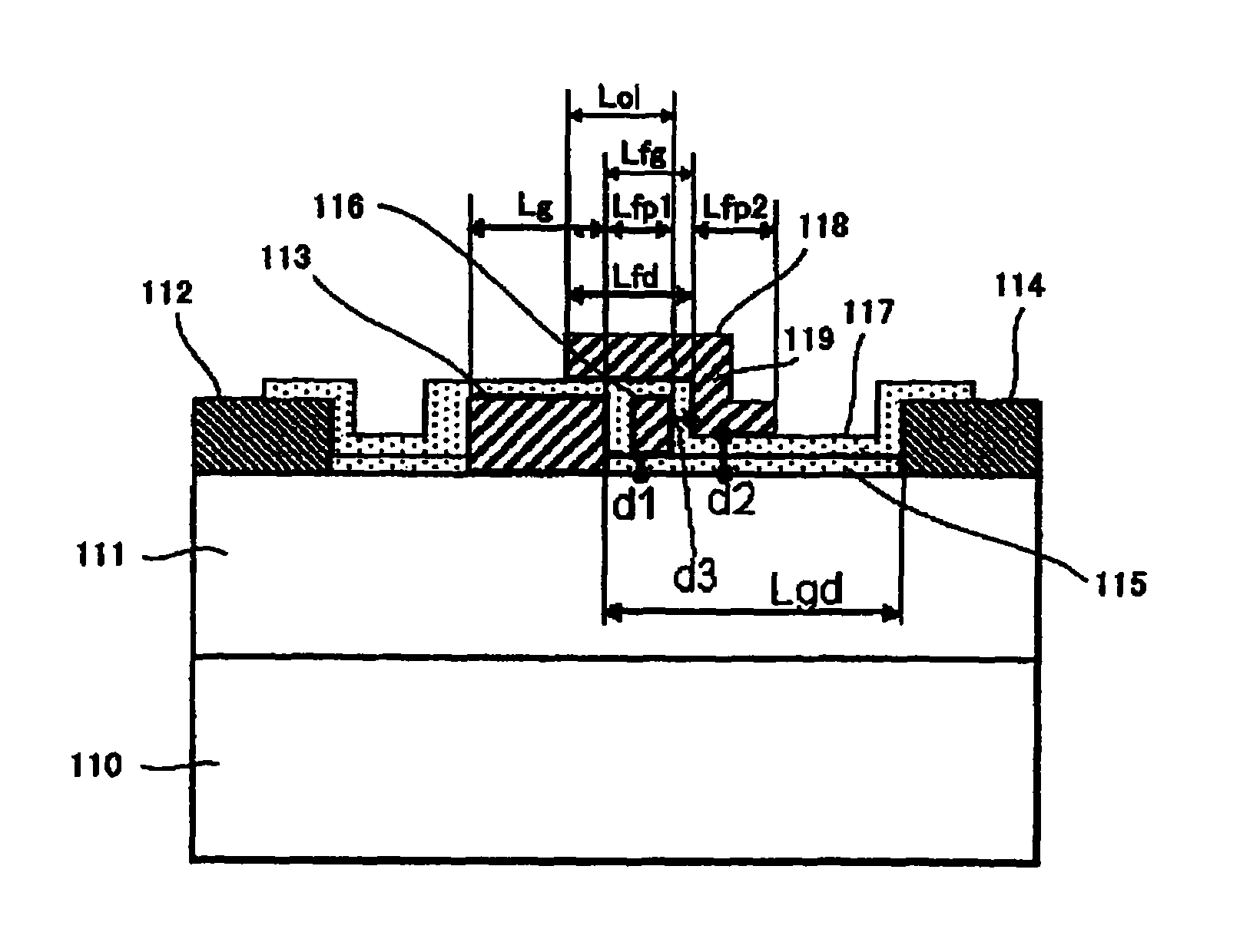
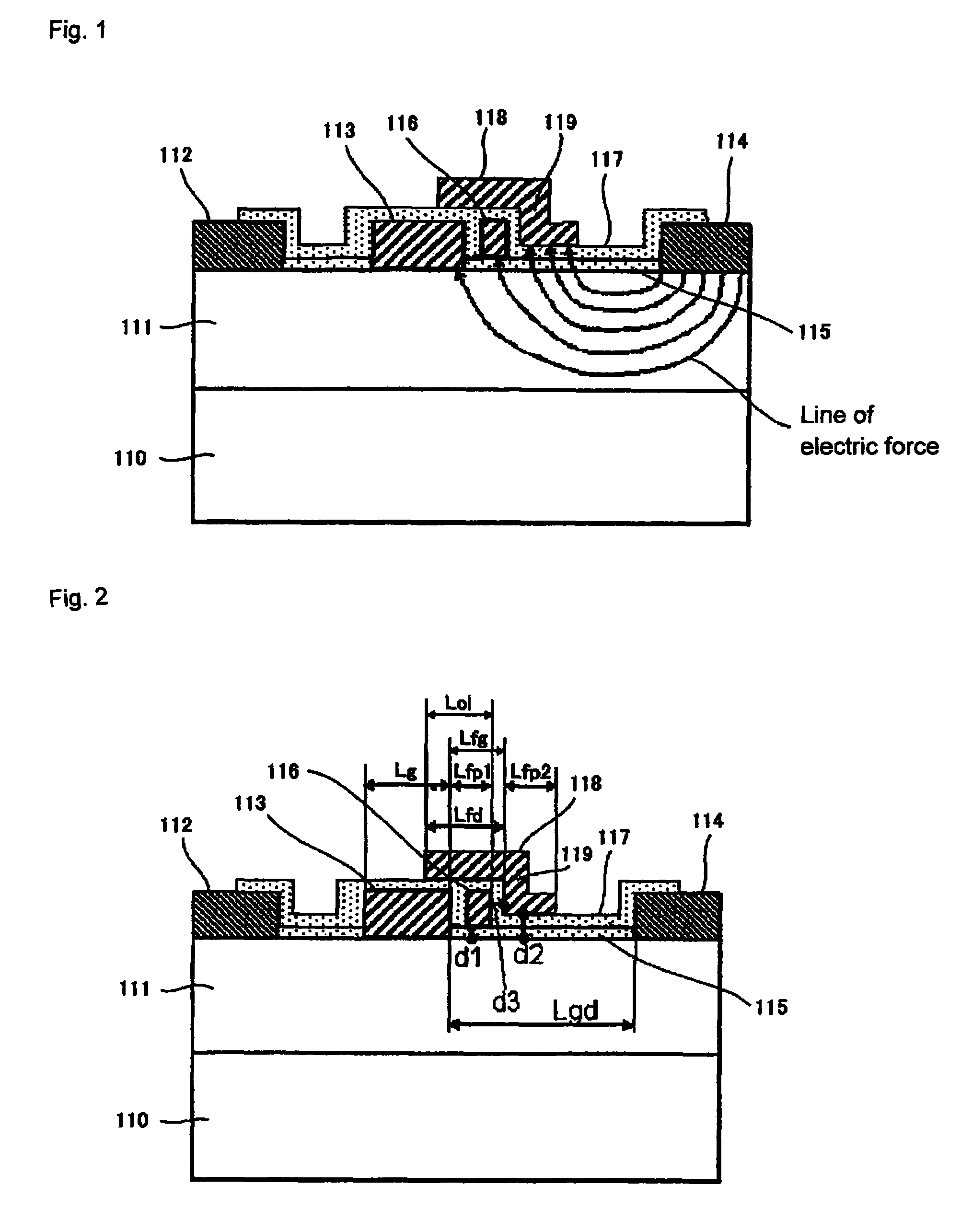
[0085]FIG. 1 is a cross sectional view showing the structure of a field effect transistor of the present exemplary embodiment. The field effect transistor shown in FIG. 1 comprises a dual field plate structure.

[0086]This transistor comprises a semiconductor substrate 110 made of GaN or InP, a layer structure made of compound semiconductor (compound semiconductor 111) provided on the semiconductor substrate 110, a source electrode 112 and a drain electrode 114 which are formed on the upper part of the compound semiconductor 111 in a spaced manner, a gate electrode 113 placed between the source electrode 112 and the drain electrode 114, a first field plate (first field plate electrode 116) provided above the semiconductor substrate 110 in the region between the gate electrode 113 and the drain electrode 114 and isolated from the compound semiconductor 111 (semiconductor substrate 110), and a second field plate (second field plate electrode 118) provided above the compound semiconducto...

second exemplary embodiment

[0144]While explanation has been made in the first exemplary embodiment by taking an example of the case where there is employed the structure in which the gate electrode 113 and the first field plate electrode 116 are structurally separated, and are electrically connected in the isolation region of the device, there may be employed an integral structure in which the gate electrode 113 and the first field plate electrode 116 are integrally formed in a continuous shape.

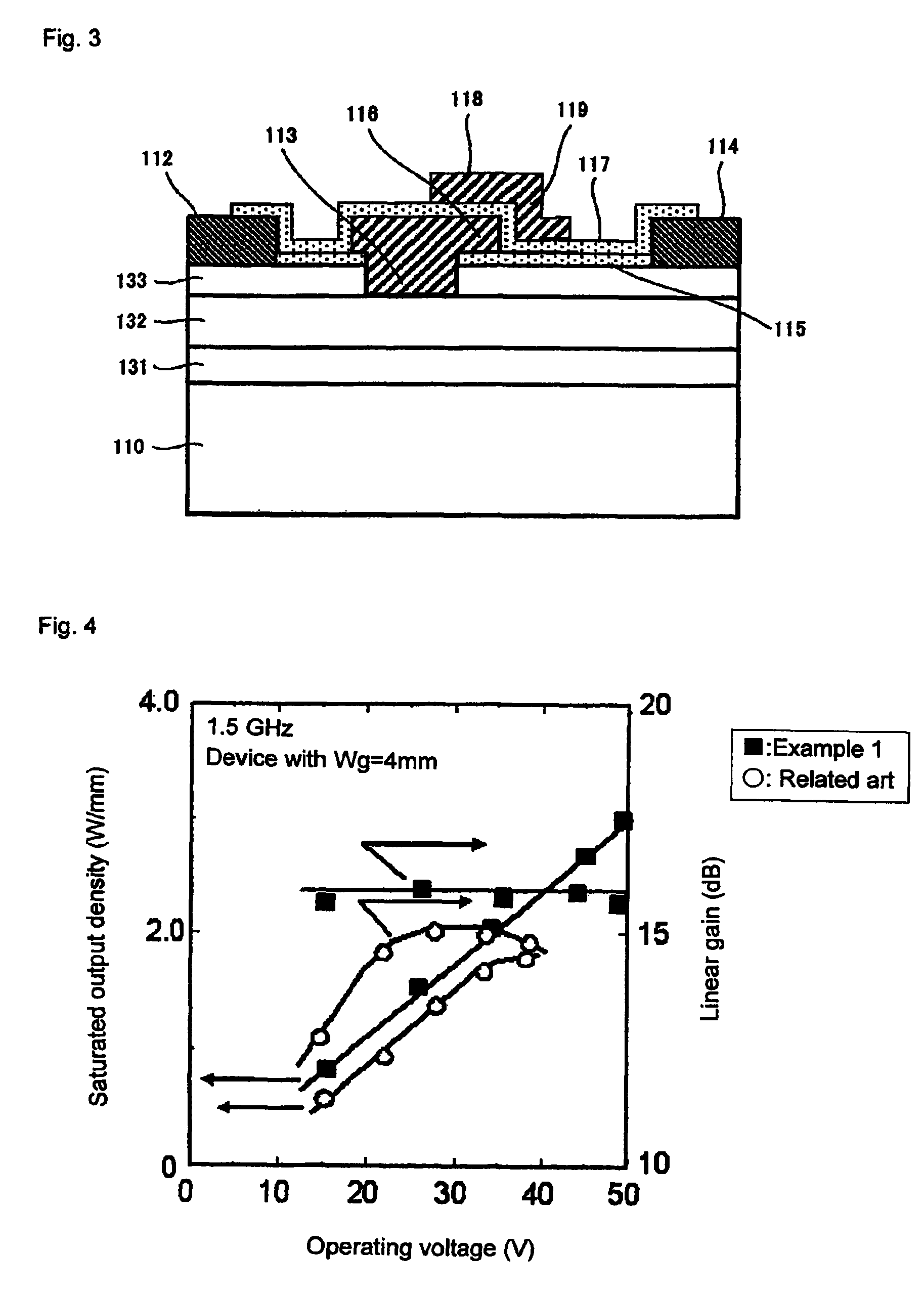
[0145]FIG. 3 is a cross sectional view showing the structure of a field effect transistor of the present exemplary embodiment.

[0146]The fundamental structure of the field effect transistor shown in FIG. 3 is very similar to that of the field effect transistor (FIG. 1) disclosed in the first exemplary embodiment, but the first field plate electrode 116 is constructed in a manner that it is integrally continuous to the gate electrode 113. It is to be noted that “integrally continuous” refers herein to the state formed in...

third exemplary embodiment

[0148]In the aforementioned exemplary embodiments, explanations have been made for the cases of the structure in which the lower surface of the first field plate electrode 116 is located on the side of the compound semiconductor 111 relative to the lower surface of the shielding part 119. In the field effect transistors illustrated in the aforementioned exemplary embodiments, there may be also employed a structure in which the lower surface of the shielding part 119 is located at the lower part relative to the lower surface of the first field plate electrode 116, i.e., on the compound semiconductor 111 side. In the present exemplary embodiment, explanation will be made by taking an example of the case of the transistor similar to that disclosed in the second exemplary embodiment.

[0149]FIG. 11 is a cross sectional view showing the structure of the field effect transistor of the present exemplary embodiment.

[0150]In the field effect transistor shown in FIG. 11, the lower end of the sh...


PUM


Abstract

A field effect transistor includes a layer structure made of compound semiconductor (111) provided on a semiconductor substrate (110) made of GaAs or InP, as an operation layer, and employs a first field plate electrode (116) and a second field plate electrode (118). The second field plate electrode includes a shielding part (119) located in the region between the first field plate electrode and a drain electrode (114), and serves to shield the first field plate electrode from the drain electrode. When, in the cross sectional view in the gate length direction, the length in the gate length direction of an overlap region, in which the second field plate electrode overlaps the upper part of a structure composed of the first field plate electrode and a gate electrode (113), is designated as Lol, and the gate length is Lg, the relation expressed as 0≦Lol / Lg≦1 holds.

Description

TECHNICAL FIELD[0001]The present invention relates to a field effect transistor. In particular, the present invention relates to a structure for attaining excellent high frequency characteristic and high voltage performance in a hetero-junction field effect transistor utilizing III-V compound semiconductor provided on a semiconductor substrate made of GaAs or InP.RELATED ART[0002]As a Field Effect Transistor (hereinafter referred to as “FET” as occasion may demand) using compound semiconductor, there conventionally exists a FET as shown in FIG. 17 (Non-Patent Document 1: K. Asano, et al., 1998 International Electron Devices Meeting Digest (IEDM 98) pp. 59-62). FIG. 17 is a cross sectional view showing a structure of a Hetero-Junction Field Effect Transistor (which will be referred to as HJFET hereinafter) included in conventional type of transistors.[0003]In this HJFET, a buffer layer 211 is formed on a GaAs substrate 210, and a GaAs operation layer 212 is formed on the buffer layer...

Claims


Application Information

Patent Timeline
Patent Type & Authority Patents(United States)
IPC IPC(8): H01L29/812H01L21/338
CPCH01L29/404H01L29/7783H01L29/7787H01L29/802H01L29/812
Inventor MIYAMOTO, HIRONOBUANDO, YUJIOKAMOTO, YASUHIRONAKAYAMA, TATSUOINOUE, TAKASHIOTA, KAZUKIWAKEJIMA, AKIOKASAHARA, KENSUKEMURASE, YASUHIROMATSUNAGA, KOHJIYAMANOGUCHI, KATSUMISHIMAWAKI, HIDENORI
Owner NEC CORP
Why Eureka
Try Eureka