Integrated high frequency BALUN and inductors

a high-frequency balun and inductors technology, applied in the field of semiconductor integrated circuits, can solve the problems of low quality, limited integration, and inability to address the capacitive coupling between primary and secondary windings

Active Publication Date: 2010-10-05
THETA IP
View PDF13 Cites 24 Cited by
  • Summary
  • Abstract
  • Description
  • Claims
  • Application Information

AI Technical Summary

Problems solved by technology

Carpentier suggests an implementation of a BALUN transformer that has five metallization layers, therefore requiring a complex manufacturing process having many layers often restricting conductor routing over the BALUN transformer.
However, the issue of capacitive coupling between the primary and secondary windings is not addressed, as the windings are essentially positioned such that a maximum capacitive coupling is achieved, having a disadvantage in operation at high frequencies, for example several GHz, as the capacitive coupling will tend to short-circuit the BALUN at these higher frequencies.
However, such integration has been limited due to flux leakage, capacitive coupling limits, and significant series resistance.
While coplanar interleaved transformers reduce size and are widely used, they suffer from low quality (Q) factor, small coupling coefficients, and, if used as a BALUN, the center tap is often at an undesirable location, resulting in an asymmetric geometry.
As is known, asymmetry of a transformer winding causes an imbalance in the resulting differential signal and / or an imbalance in the resulting single ended signal from a differential signal.
The advent of nm-scale CMOS RFIC design poses new challenges in the design of cost-effective integrated telecommunication transceivers.
On the other hand, real estate is much more expensive in advanced sub-micron processes such as 90 nm or—even worse—in a 65 nm technology node so the design of area effective integrated inductors becomes imperative.
The conventional multi-layer inductor structure however, suffers from low self-resonance frequency mainly due to the increased inter layer parasitic capacitance: metal segments running on different layers form excellent Metal-Insulator-Metal structures that drastically affect the electrical behavior of the integrated inductor.
While desired values may be calculated based on this solution it suffers from the limitations of the conventional multi-layer inductor structure.

Method used


Image

  • Integrated high frequency BALUN and inductors
  • Integrated high frequency BALUN and inductors
  • Integrated high frequency BALUN and inductors

Examples


Embodiment Construction

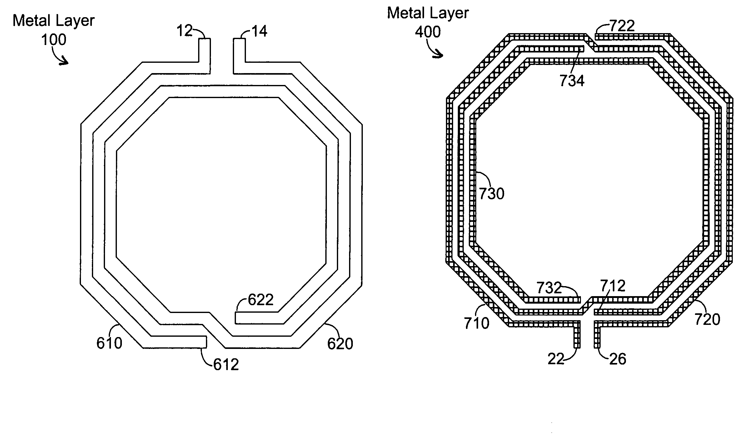
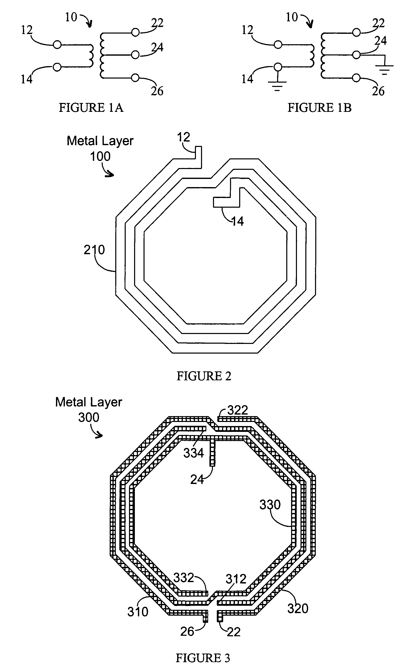
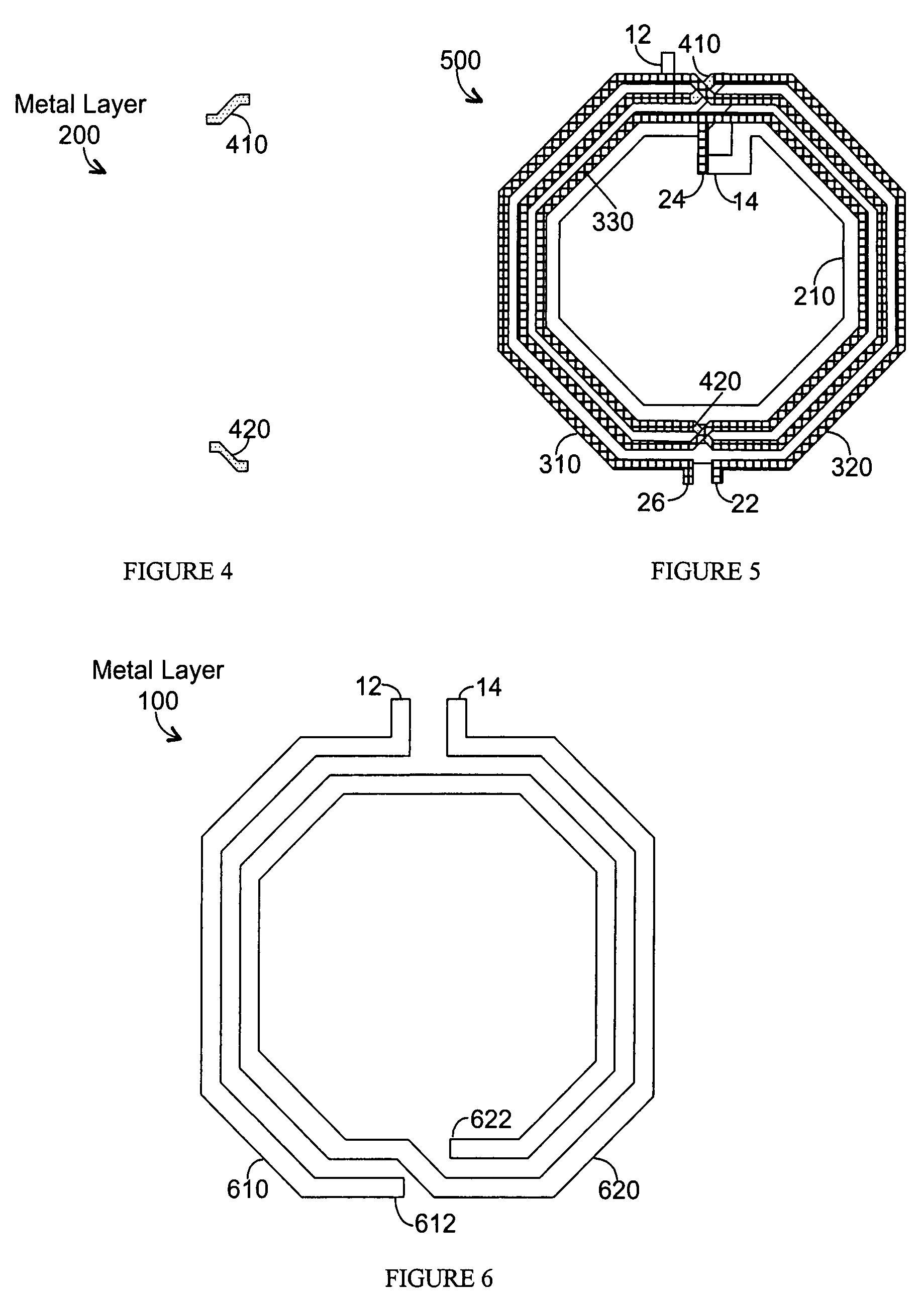
[0028]Deficiencies of the prior art have lead to a need to provide BALUN transformers that are more efficient in their design, particularly in the number of metallization layers used for their implementation without significantly adversely affecting the BALUN transformer performance. The solution of the present invention accomplishes this target by having the windings of the primary inductor in one metal layer and the windings of the secondary inductors in another metal layer not only vertically separated from, but also horizontally displaced from the first metal layer. The displacement reduces the capacitive coupling between the primary and secondary coils. Furthermore, the implementations shown enable the use of only three or four layers of metal for a BALUN transformer. It should be noted that the displacement should be such that a substantial magnetic coupling between the primary and secondary inductors of the BALUN is still achieved to ensure the proper performance of the BALUN...


PUM

PropertyMeasurementUnit
diameteraaaaaaaaaa
diameteraaaaaaaaaa
path widthaaaaaaaaaa

Abstract

Integrated high frequency balanced-to-unbalanced transformers and inductors suitable for operation in high frequencies, such as radio frequencies. Embodiments disclosed give consideration to issues related to the layout of the top and bottom inductors for the minimization of capacitive effects between layers. A displacement between the conductive paths of the top inductor and the bottom inductor is shown that provides for superior performance over prior art solutions.

Description

CROSS-REFERENCE TO RELATED APPLICATION[0001]This application is a continuation-in-part of U.S. patent application Ser. No. 11 / 208,979 filed Aug. 22, 2005, now U.S. Pat. No. 7,253,712 now allowed, entitled “Integrated High Frequency Balanced-to-Unbalanced Transformers”, which claims the benefit of U.S. Provisional Patent Application No. 60 / 605,511 filed Aug. 31, 2004.BACKGROUND OF THE INVENTION[0002]1. Field of the Invention[0003]The present invention relates to semiconductor integrated circuits, and more particularly to integrated circuit inductors that are magnetically-coupled for the purpose of creating a high frequency transformer.[0004]2. Prior Art[0005]In wireless communications, an antenna is commonly coupled, typically by means of passive components, to a transformer. In many cases, a balanced-to-unbalanced (BALUN) transformer is used. Such a transformer allows the conversion of a single-ended signal into a differential signal and vice versa. In wireless communications, the a...

Claims


Application Information

Patent Timeline
Patent Type & Authority Patents(United States)
IPC IPC(8): H01F5/00
CPCH01F27/2804H03H7/42H01L23/5227H01F17/0013H01F2017/0086H01F2027/2809Y10T29/4902H03H2001/0064Y10T29/49073Y10T29/49071H01L2924/0002H01L2924/00
Inventor PAPANANOS, YANNIS
Owner THETA IP
Why Eureka
Try Eureka