RF amplifying device

a technology amplifier, which is applied in the direction of amplifiers with semiconductor devices/discharge tubes, amplifiers with coupling networks, dual/triple band amplifiers, etc., can solve the problems of large current-carrying capacity and high q factor of rf choke inductor, large occupied area of spiral coils, over semiconductor chips or interconnection substrates, etc., to achieve high q factor, low parasitic resistance, and large current-carry

Active Publication Date: 2010-11-02
RENESAS ELECTRONICS CORP
View PDF2 Cites 11 Cited by
  • Summary
  • Abstract
  • Description
  • Claims
  • Application Information

AI Technical Summary

Benefits of technology

[0015]Further, as is well known, for supplying transmission power at a low power supply voltage to a 50-Ω antenna of mobile communications equipment such as a cellular telephone, and so forth, an impedance matching circuit is coupled between an output of the RF power amplifier, and the antenna as the load thereof. By use of, for example, a lossless transformer having a transformation ratio of 1:4 as the impedance matching circuit, a peak-to-peak amplitude at 5 V of the RF power amplifier will be turned to a peak-to-peak amplitude at 20 V. In other words, with the use of the transformer as the impedance matching circuit, load impedance can be effectively converted lower in value, so that it is possible to output a target transmission power even at a limited amplitude outputted by the RF power amplifier.
[0020]Accordingly, due to impedance conversion from the secondary line Lin of the transmission line transformer TLT to the main line Lout, conversion output power of the power hetrojunction bipolar transistor (HBT) Q can be generated from the other end Out (A) of the main line Lout of the transmission line transformer TLT. That is, a characteristic impedance is developed by the agency of the interlayer dielectric disposed between the secondary line Lin of the transmission line transformer TLT and the main line Lout. Accordingly, an inductive-capacitive coupling energy is transmitted in a transmission line mode from the secondary line Lin of the transmission line transformer TLT to the main line Lout. Therefore, it becomes possible to take out an RF amplified voltage signal from an output electrode of an amplifier element without the use of an air-core coil as a load circuit, and without the use of a spiral coil, or choke inductance, having a large current-carrying capacity and a high Q factor.
[0021]The power hetrojunction bipolar transistor (HBT) Q is formed over an III-V group compound semiconductor chip, and for the power hetrojunction bipolar transistor (HBT) Q, use is made of a hetrojunction bipolar transistor of, for example, GaAs, and InP. Further, as another HBT, use can be made of an SiGe hetrojunction bipolar transistor formed over a silicon substrate, as well. Accordingly, the collector output electrode of the power hetrojunction bipolar transistor (HBT) Q is formed of an interconnection layer CBP fabricated on the surface of the III-V group compound semiconductor chip, or on the surface of a silicon semiconductor chip by a semiconductor manufacturing process. The collector output electrode CBP of the power hetrojunction bipolar transistor (HBT) Q is coupled to a joint CP of the main line Lout as the upper-level interconnection formed over the main surface of the circuit board CB of the RF power module via four bonding wires BW coupled in parallel. Low parasitic resistance and low parasitic inductance, caused by the four bonding wires BW coupled in parallel, will reduce a voltage drop owing to a collector current of the power hetrojunction bipolar transistor (HBT) Q on the order of an ampere. In this connection, the joint CP of the main line Lout as the upper-level interconnection is a bonding pad for the four bonding wires BW.
[0022]That is, the joint CP of the bonding pad is formed so as to be isolated from an energy transmission / coupling part for inductive-capacitive coupling, located between the transmission line of the main line Lout, and the transmission line of the secondary line Lin of the transmission line transformer TLT. A first reason as the main reason for isolation described as above is to lessen effects of magnetic fluxes of an RF frequency generated from the four bonding wires BW coupled to the joint CP of the bonding pad on the energy transmission coupling part between the transmission line of the main line Lout, and the transmission line of the secondary line Lin, of the transmission line transformer TLT. A second reason for the isolation is to lesson effects of mechanical pressure exerted by a wire bonder in the step of wire bonding with the bonding wires BW at the time of manufacturing the RF power module on the interlayer dielectric disposed between the secondary line Lin, and the main line Lout, of the transmission line transformer TLT. That is, taking into consideration a possibility of a crack occurring to the interlayer dielectric due to the pressure exerted by the wire bonder, or electrical insulation properties of the interlayer dielectric undergoing deterioration due to occurrence of a crack, the joint CP of the bonding pad is formed so as to be isolated from the energy transmission coupling part.
[0040]That is, a condition for impedance matching of the transmission line transformer can be maintained when the output electrode of the power transistor in the final amplifying stage is joined with the transmission line transformer serving as the impedance matching circuit.

Problems solved by technology

However, a large current-carrying capacity and a high Q factor are required of the RF choke inductor.
In order to attain the large current-carrying capacity and the high Q factor, however, a problem is encountered in that an occupied area of a spiral coil, over a semiconductor chip or a multi-level interconnection substrate, is large in size.

Method used


Image

  • RF amplifying device
  • RF amplifying device
  • RF amplifying device

Examples


Embodiment Construction

Representative Embodiment of the Invention

[0055]First, the overview of a representative embodiment of the invention, disclosed under the present application, is described hereinafter. It is to be understood that a reference numeral inside the parentheses, referred to in the drawings, in description of the overview of the representative embodiment of the invention, simply indicates what is included in the concept of a constituent element with the reference numeral affixed thereto, by way of example.

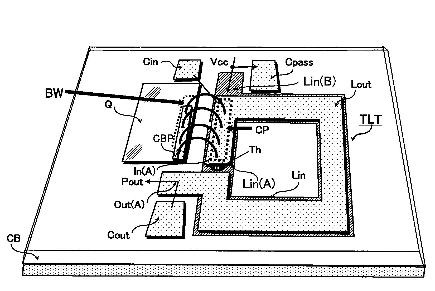
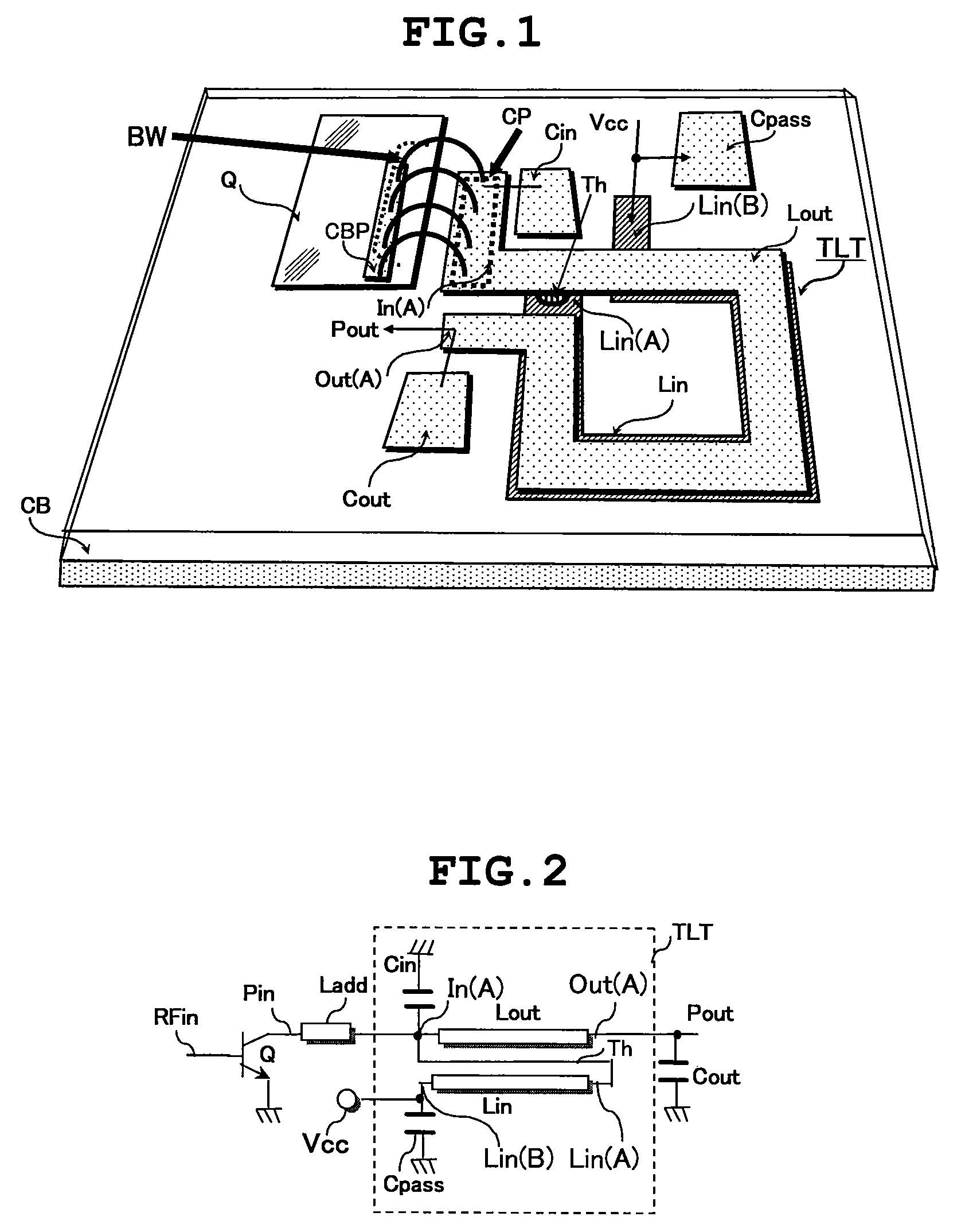
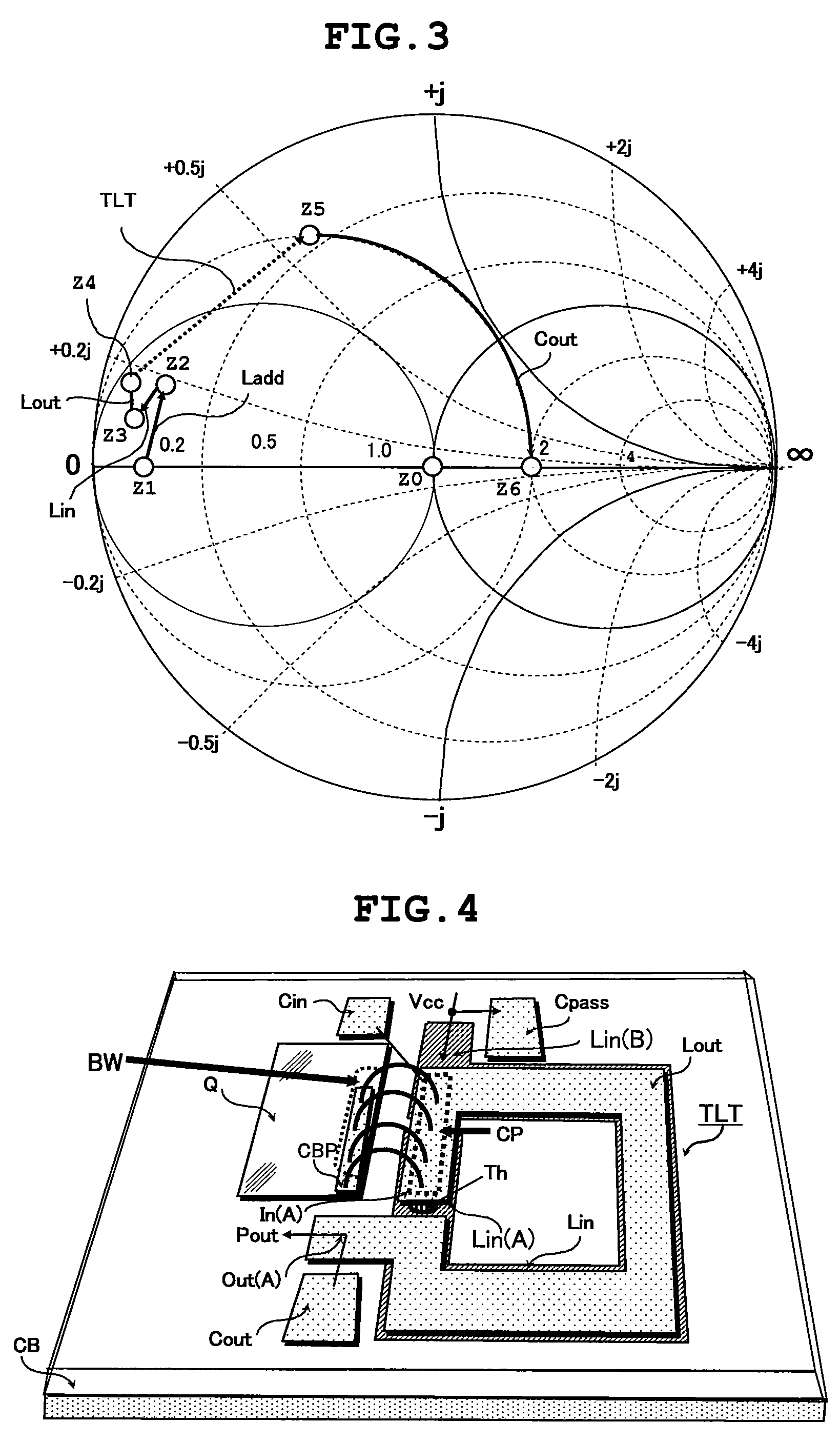
[0056][1] An RF amplifying device according to the representative embodiment of the invention comprises a power transistor (Q) for generating transmission power to be fed to an antenna of a wireless device, and a transmission line transformer (TLT) coupled to an output electrode (CBP) of the power transistor.

[0057]The transmission line transformer includes a main line (Lout), and a secondary line (Lin). The transmission power from the output electrode of the power transistor is fed to one ...


PUM


Abstract

An RF amplifying device includes a transmission line transformer coupled to an output electrode of a power transistor for generating transmission power to be fed to an antenna. The transmission power from the output electrode of the power transistor is fed to one end of a main line of the transmission line transformer, and one end of a secondary line of the transmission line transformer is coupled to an AC grounding node. The other end of the secondary line is coupled to the one end of the main line, thereby generating the transmission power. Coupling energy is transmitted from the secondary line to the main line. Coupling members electrically coupled to the output electrode of the power transistor are electrically coupled to a joint formed in either the main line, or the secondary line, at part of the energy coupling part.

Description

CLAIM OF PRIORITY[0001]The present application claims priority from Japanese patent application JP 2007-253391 filed on Sep. 28, 2007, the content of which is hereby incorporated by reference into this application.FIELD OF THE INVENTION[0002]The invention relates to an RF (radio frequency) amplifying device having a transmission line type matching circuit, and in particular, to a technology useful in maintaining a condition for impedance matching upon coupling an output electrode of a power transistor in the final amplifying stage with a transmission line transformer serving as an impedance matching circuit.BACKGROUND OF THE INVENTION[0003]A plurality of communication systems are included in mobile communications as represented by a cellular telephone. For example, in Europe, there exists W-CDMA as a third generation communication system that has recently started its service in addition to GSM prevalent as a second generation communication system, and EDGE at a transmission rate enh...

Claims


Application Information

Patent Timeline
Patent Type & Authority Patents(United States)
IPC IPC(8): H03F3/213
CPCH03F1/565H03F3/602H03F2200/111H03F2200/423H03F2200/429H03F2200/451H03F2200/537H03F2200/541
Inventor OHNISHI, MASAMITANAKA, RYOUICHI
Owner RENESAS ELECTRONICS CORP
Why Eureka
Try Eureka