Fluxless reflow process for bump formation

a fluxless reflow and bump technology, applied in the direction of welding/cutting media/materials, manufacturing tools, solventing apparatus, etc., can solve the problems of fluxless reflow for bump formation, increased cost of solder bump formation, and new defects can be introduced during the cleaning process, so as to achieve simplified processes and easy setting of apparatus operation parameters

Active Publication Date: 2010-11-23
SEMICON MFG INT (SHANGHAI) CORP
View PDF11 Cites 0 Cited by
  • Summary
  • Abstract
  • Description
  • Claims
  • Application Information

AI Technical Summary

Benefits of technology

[0027]1. In the embodiments of the present invention, the reflow process has been divided into three steps, and the solder keeps in a melting or half-melting state for 120 s-540 s during the first purifying process, so that the escapable organic material in the solder and the gas molecules contained therein may escape slowly, thus splashing can be avoided in the following ball-forming process and the problem of forming solder balls around bumps can also be avoided.
[0028]2. In the embodiments of the present invention, the purifying process is a process in which the temperature increases from Tc−4° C. to Tc+4° C., so that the impurities and evaporable materials in the solder can escape from the solder effectively without splashing.
[0029]3. In the embodiments of the present invention, the purifying process includes three temperature-constant stages each having a duration of 40 s to 180 s. As a result, the operation parameter of the apparatus can be set easily and the processes may be simplified.
[0030]4. The embodiments of the present invention also provide another fluxless reflow process for bump formation including: a first reflow; a first bump cleaning after the first reflow for removing residual organic metal salt and oxide on the surface of bumps as well as other contaminations which have not been removed in the first reflow; and a second reflow for repairing the surfaces of bumps which are rough due to many ostioles resulted from the first cleaning which do not meet the requirement of quality, in order to form the bumps with smooth surfaces and desirable shapes.

Problems solved by technology

Since the flux is expensive in price and a cleaning process is also required after bump formation, the above described process wastes the resources, and the cost of the solder bump formation is increased.
Moreover, new defects can be introduced during the cleaning process because the flux may react with the flux removing material.
Therefore, a fluxless reflow for solder formation is emerging as a challenging and competitive process.
However, the above method can only be used to the reflow in chip interconnection.

Method used


Image

  • Fluxless reflow process for bump formation
  • Fluxless reflow process for bump formation
  • Fluxless reflow process for bump formation

Examples


embodiment 1

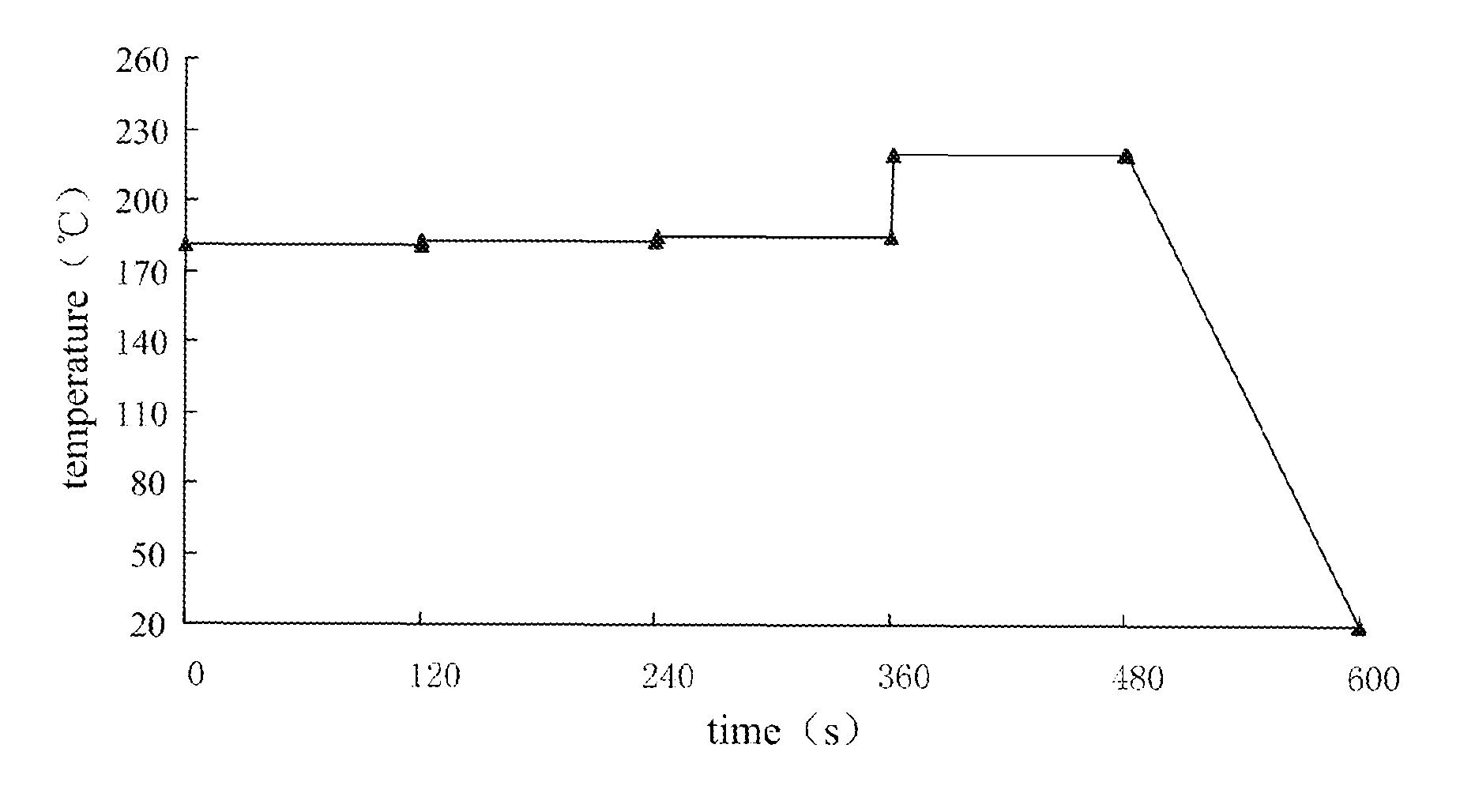
[0052]FIG. 5 shows a temperature profile of the eutectic lead-tin alloy (37 wt % Pb, 63 wt % Sn) according to the embodiment 1 of the present invention. In the preferred embodiment of the present invention, the eutectic lead-tin alloy is employed. The purifying process is divided into three temperature-constant stages, the temperatures of which are 181° C., 183° C. and 185° C. respectively, each having a duration of 120 s. The purifying process is performed in an atmosphere of formic acid gas. Next, the eutectic lead-tin alloy is reflowed at a temperature of 220° C. for 100 s in an atmosphere of formic acid gas. Then, the temperature is lowered to the room temperature naturally in a nitrogen atmosphere to form a bump of eutectic lead-tin alloy.

embodiment 2 to embodiment 4

[0053]For the detailed process parameters in embodiments 2 to 4, refer to the above description of embodiment 1. The detailed process parameters are as shown in table 1.

[0054]

TABLE 1The detailed process parameters of the eutectic lead-tin alloy in embodiments 2 to 4The purifying processThe ball-formingStage 1Stage 2Stage 3processThe cooling processTemperaturetimeTemperaturetimeTemperaturetimeTemperaturetimeTemperatureembodiment(° C.)(s)(° C.)(s)(° C.)(s)(° C.)(s)(° C.)Atmosphereembodiment 217912018114018316021012020nitrogenembodiment 318010018312018514022010025embodiment 4183 80185100187120240 8025

embodiment 5 to embodiment 7

[0055]For example, a silver-tin alloy with 2.5 wt % Ag and 97.5 wt % Sn is used to form bumps of the silver-tin alloy.

[0056]The detailed process parameters are as shown in table 2.

[0057]

TABLE 2The detailed process parameters of silver-tin alloy with 2.5 wt % Ag and 97.5 wt % Sn inembodiments 5 to 7The purifying processThe ball-formingStage 1Stage 2Stage 3processThe cooling processTemperaturetimeTemperaturetimeTemperaturetimeTemperaturetimeTemperatureembodiment(° C.)(s)(° C.)(s)(° C.)(s)(° C.)(s)(° C.)atmosphereembodiment 521750219180221902359025nitrogenembodiment 6215602171102191302506025embodiment 72131402151002171602604525

[0058]For most types of solder, bumps with a smooth surface and without bubbles can be formed by the above reflow process. During this fluxless reflow process for bump formation, no splashing occurs and no solder balls are formed around the bumps.

[0059]For some types of solder with a high content of contamination, however, there may still be some un-evaporated ma...


PUM

PropertyMeasurementUnit
temperatureaaaaaaaaaa

Abstract

A fluxless reflow process for bump formation is provided, which includes: a purifying process for keeping solder in a state of melting or half-melting for 40 s to 540 s; a ball-forming process for melting the solder completely to form ball-like bumps; and a cooling process. The splashing of solder can be avoided and the defect that there may be solder balls around the bumps can be eliminated.

Description

[0001]This application claims the priority of Chinese Patent Application No. 200610119047.5, filed Dec. 4, 2006, the entire disclosure of which is incorporated herein by reference.FIELD OF THE INVENTION[0002]The present invention relates to a semiconductor chip package process, and more particularly, to a fluxless reflow process for bump formation.BACKGROUND OF THE INVENTION[0003]With the development of integrated circuits (ICs), electronic products tend to become more and more smaller in size, more and more intelligent, with a high performance and a high reliability. The smaller dimension and higher integration of IC present a higher requirement to the IC package technique.[0004]The flip chip is a technique in which a chip is flipped over and then connected with a board by solder balls formed on the surface of the chip so as to reduce the package size. The flip chip technology may satisfy the requirement for high performance (such as, high speed, high frequency and smaller pins) wi...

Claims


Application Information

Patent Timeline
Patent Type & Authority Patents(United States)
IPC IPC(8): H01L21/4763
CPCB23K3/0623H01L24/11H01L2924/01322H01L2924/14H01L2224/05026H01L2224/05568H01L2224/05023H01L2224/05572H01L2224/056H01L2224/1181H01L24/05H01L2924/00H01L2924/00014
Inventor WANG, TSING-CHOWLI, RUNLING
Owner SEMICON MFG INT (SHANGHAI) CORP
Why Eureka
Try Eureka