
Chemical trim of photoresist lines by means of a tuned overcoat material

a technology of photoresist line and overcoat, which is applied in the direction of photosensitive materials, instruments, photomechanical equipment, etc., can solve the problems of too much activation of resist, too much reduction in linewidth, and acid will not provide sufficient activation of resist to provide enough reduction in resist linewidth. , to achieve the effect of superior linewidth control and reducing the linewidth of an imag

Inactive Publication Date: 2011-01-04
GLOBALFOUNDRIES U S INC
View PDF13 Cites 24 Cited by
  • Summary
  • Abstract
  • Description
  • Claims
  • Application Information

AI Technical Summary

Benefits of technology

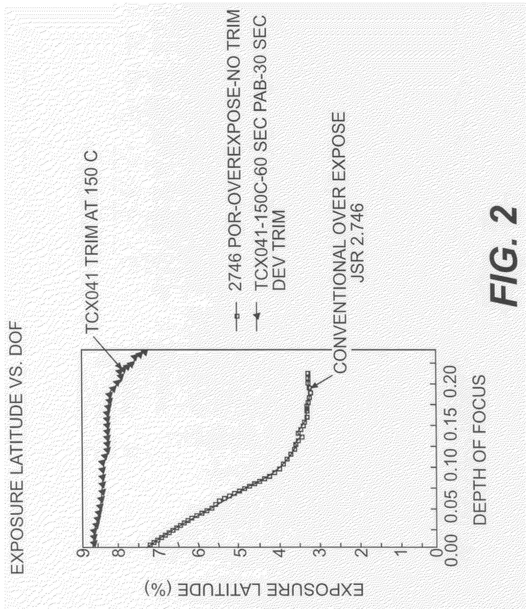
This process effectively reduces linewidth while maintaining a wider process window, providing superior linewidth control and preventing degradation of the resist pattern, as demonstrated by increased exposure latitude and focus depth, enabling more manufacturable lithographic processes.

Problems solved by technology

Too strong an acid will cause too much activation of the resist, and too much consequent reduction in linewidth.
Too weak an acid will not provide sufficient activation of the resist to provide enough reduction in the resist linewidth.
Too much trim is undesirable, as it will degrade the resist pattern rather than simply reduce the linewidth.
Carboxylic acids are very weak acids would not have sufficient acidic strength to cleave regular acid labile moieties except acetals and ketals.

Method used


Image

  • Chemical trim of photoresist lines by means of a tuned overcoat material
  • Chemical trim of photoresist lines by means of a tuned overcoat material
  • Chemical trim of photoresist lines by means of a tuned overcoat material

Examples


Embodiment Construction

1. Field of the Invention

The field of the invention comprises formation of fine line lithography patterns for the purpose of semiconductor fabrication.

2. Background of the Invention and Related Art

Historically, lithographic scaling has generally been achieved by means of increasing the numerical aperture available for optical exposure equipment, and by means of using shorter exposure wavelengths. At present, the industry has reached a condition in which it is no longer possible to economically increase numerical aperture or reduce the exposure wavelength. As a result, many alternative methods of scaling integrated circuit lithography are being investigated. One method involves the use of multiple exposures to form a single lithographic mask pattern on the wafer. The pitch of the pattern is split by interstitially placing a line from a second mask in between two lines formed by a first mask. The effective pitch of the resulting combined pattern can be twice as dense as that of a sing...


PUM

PropertyMeasurementUnit
temperatureaaaaaaaaaa

Abstract

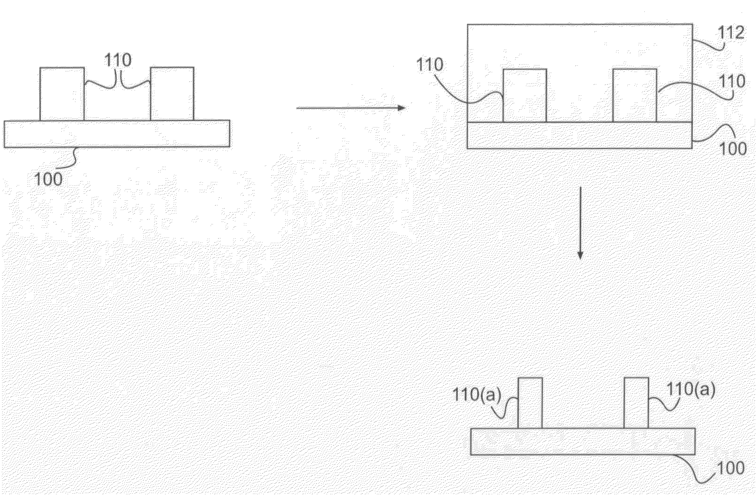
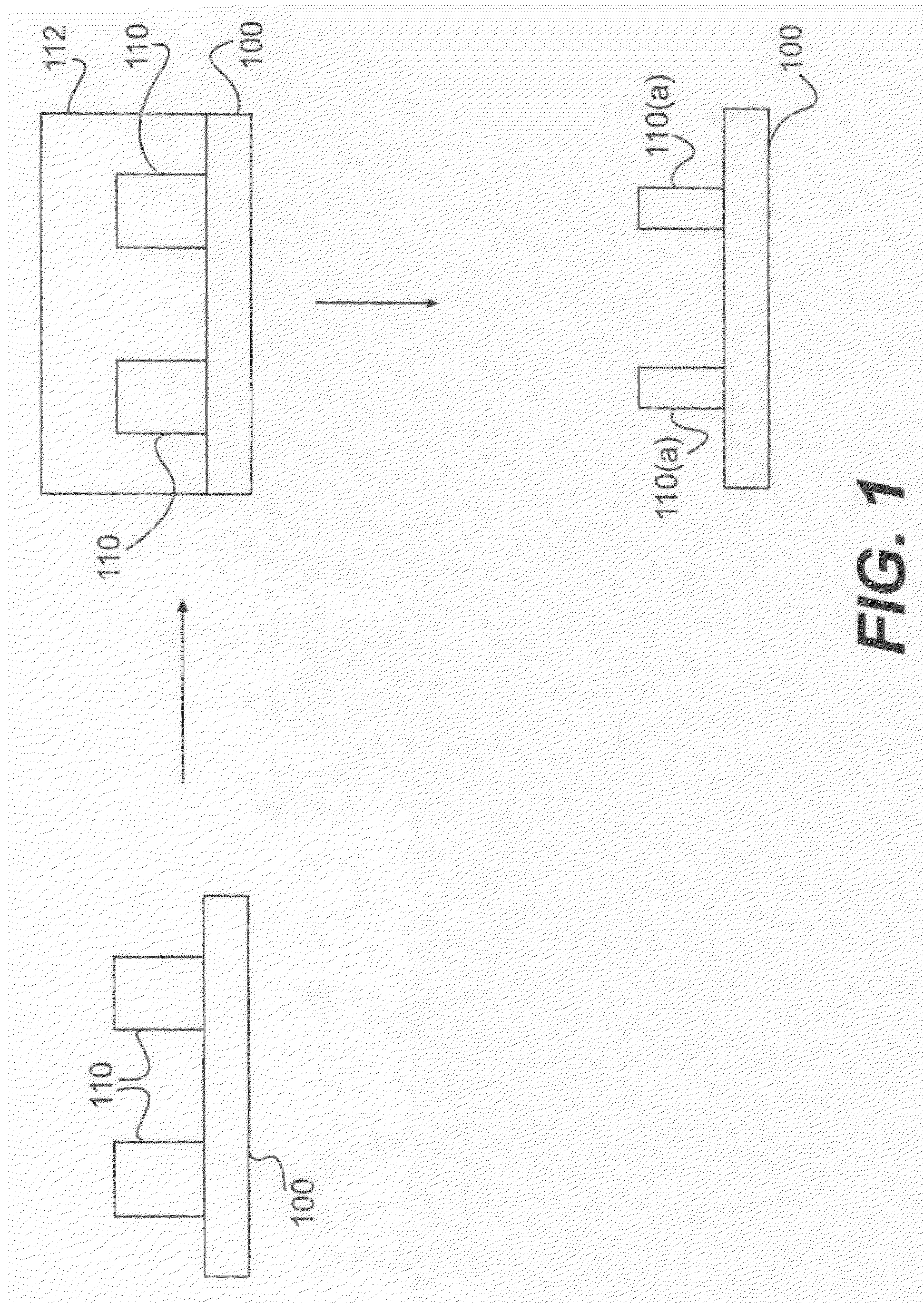
A new lithographic process comprises reducing the linewidth of an image while maintaining the lithographic process window, and using this process to fabricate pitch split structures comprising nm order (e.g., about 22 nm) node semiconductor devices. The process comprises applying a lithographic resist layer on a surface of a substrate and patterning and developing the lithographic resist layer to form a nm order node image having an initial line width. Overcoating the nm order node image with an acidic polymer produces an acidic polymer coated image. Heating the acidic polymer coated image gives a heat treated coating on the image, the heating being conducted at a temperature and for a time sufficient to reduce the initial linewidth to a subsequent narrowed linewidth. Developing the heated treated coating removes it from the image resulting in a free-standing trimmed lithographic feature on the substrate. Optionally repeating the foregoing steps further reduces the linewidth of the narrowed line. The invention also comprises a product produced by this process.

Description

DESCRIPTION OF THE INVENTION1. Field of the InventionThe field of the invention comprises formation of fine line lithography patterns for the purpose of semiconductor fabrication.2. Background of the Invention and Related ArtHistorically, lithographic scaling has generally been achieved by means of increasing the numerical aperture available for optical exposure equipment, and by means of using shorter exposure wavelengths. At present, the industry has reached a condition in which it is no longer possible to economically increase numerical aperture or reduce the exposure wavelength. As a result, many alternative methods of scaling integrated circuit lithography are being investigated. One method involves the use of multiple exposures to form a single lithographic mask pattern on the wafer. The pitch of the pattern is split by interstitially placing a line from a second mask in between two lines formed by a first mask. The effective pitch of the resulting combined pattern can be twic...

Claims


Application Information

Patent Timeline
Patent Type & Authority Patents(United States)
IPC IPC(8): G03F7/00G03F7/40G03F7/004
CPCG03F7/40Y10T428/24802
Inventor BURNS, SEAN DAVIDCOLBURN, MATTHEW E.HOLMES, STEVEN JOHNHUANG, WU-SONG
Owner GLOBALFOUNDRIES U S INC
Learn More