
Aluminum contact integration on cobalt silicide junction

a technology of silicide junction and aluminum contact, which is applied in the direction of chemical vapor deposition coating, coating, basic electric elements, etc., can solve the problems of reducing the electrical properties of small devices, tungsten resistivity nearly twice that of aluminum, and reducing the resistance of materials with less resistan

Inactive Publication Date: 2011-01-11
APPLIED MATERIALS INC
View PDF199 Cites 17 Cited by
  • Summary
  • Abstract
  • Description
  • Claims
  • Application Information

AI Technical Summary

Problems solved by technology

As device geometry shrinks, however, the tendency of silicon and aluminum to diffuse through each other degrades electrical properties of the smaller devices.
Resistivity of tungsten is nearly twice that of aluminum, however, and the smaller devices of the future will require lower resistivity materials.

Method used


Image

  • Aluminum contact integration on cobalt silicide junction
  • Aluminum contact integration on cobalt silicide junction
  • Aluminum contact integration on cobalt silicide junction

Examples


Embodiment Construction

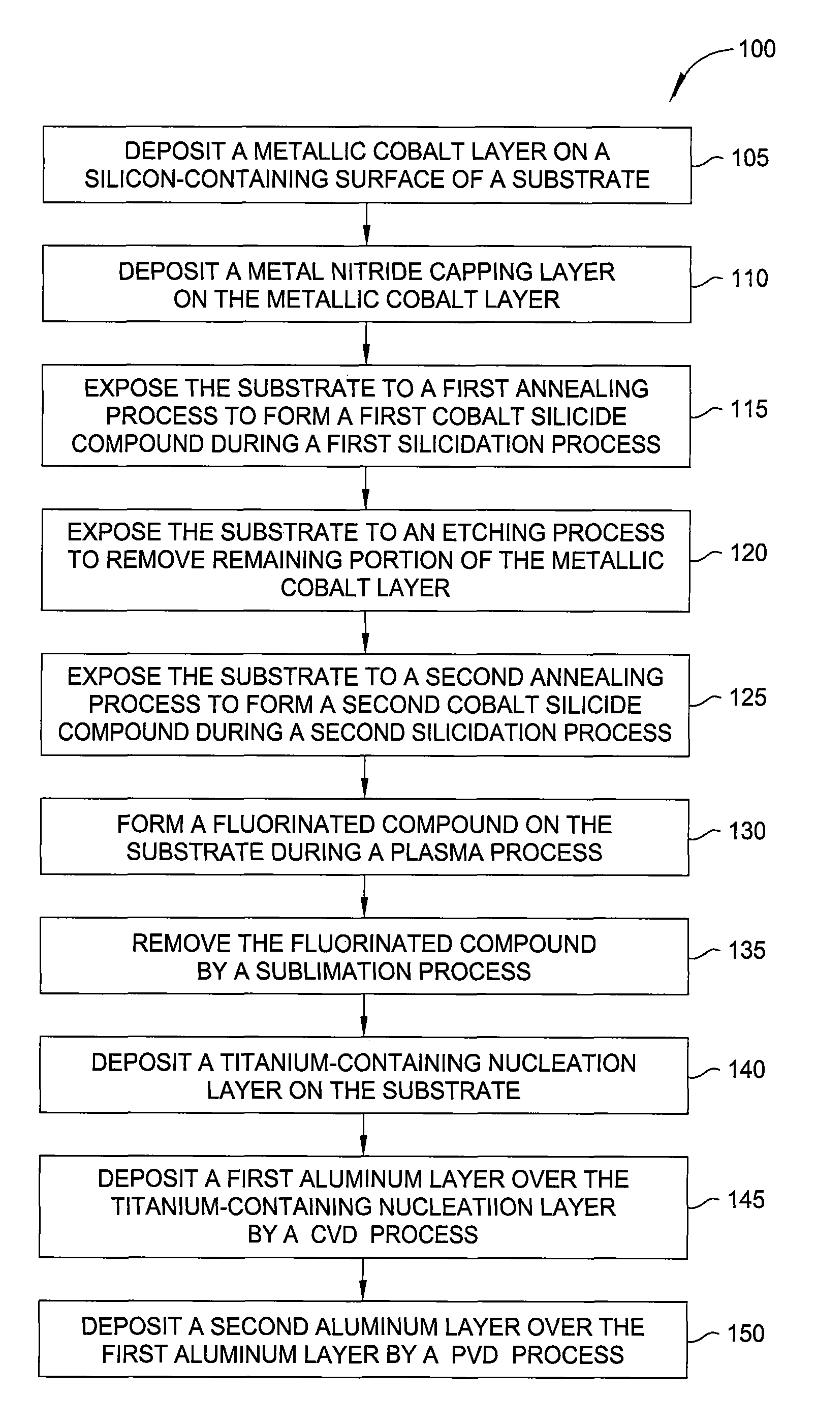
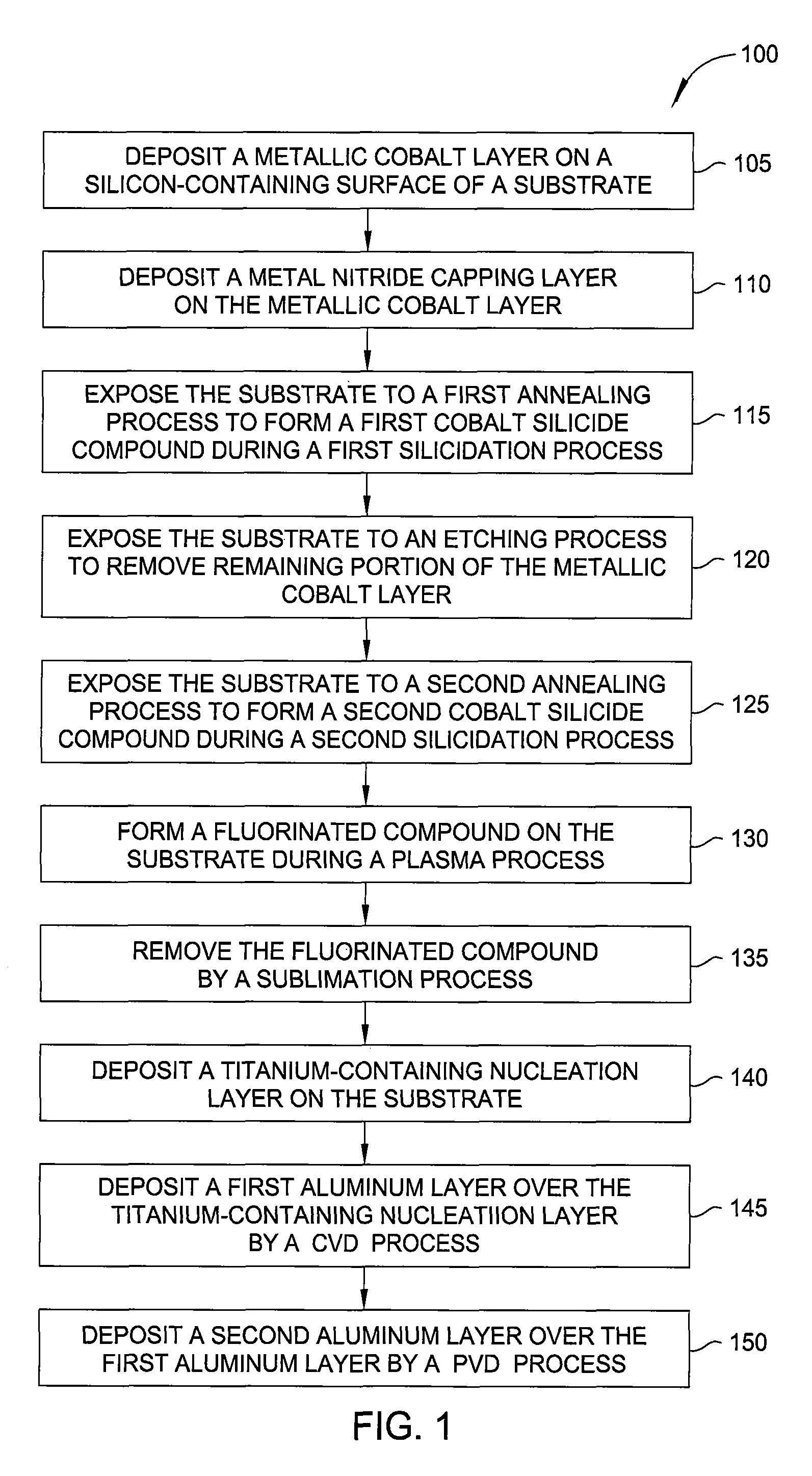
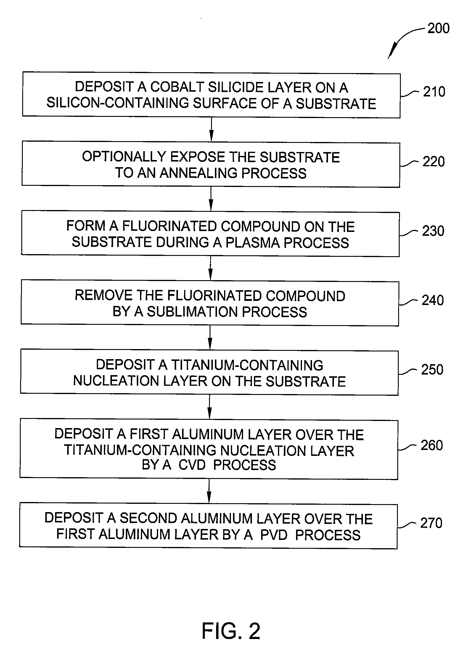
[0021]Embodiments of the invention provide a method for integrating a metal contact into a cobalt suicide region of a semiconductor device. One or more cobalt silicide regions are formed on a silicon-containing surface of a substrate. The substrate is then cleaned using a plasma process to remove surface impurities. A nucleation layer may be formed on the clean substrate. A metal contact may then be formed on the substrate. Aluminum may be used for the metal contact in this process without using a barrier layer. Not intending to be bound by theory, it has been discovered that a cobalt silicide region prepared according to embodiments described herein has sufficient barrier properties to prevent diffusion of silicon, or any other impurities, into the aluminum, without use of a resistive barrier layer.

[0022]In one embodiment, a metal contact junction may be formed by using process 100, depicted in a flow chart by FIG. 1. In step 105, a metallic cobalt layer is deposited on a silicon-c...


PUM

PropertyMeasurementUnit
temperatureaaaaaaaaaa

Abstract

Embodiments herein provide methods for forming an aluminum contact on a cobalt silicide junction. In one embodiment, a method for forming materials on a substrate is provided which includes forming a cobalt silicide layer on a silicon-containing surface of the substrate during a silicidation process, forming a fluorinated sublimation film on the cobalt silicide layer during a plasma process, heating the substrate to a sublimation temperature to remove the fluorinated sublimation film, depositing a titanium-containing nucleation layer over the cobalt silicide layer, and depositing an aluminum-containing material over the titanium-containing nucleation layer. In one example, the method further provides forming the cobalt silicide layer by depositing a cobalt-containing layer on the silicon-containing surface, heating the substrate during a rapid thermal annealing (RTA) process, etching away any remaining portions of the cobalt-containing layer from the substrate, and subsequently heating the substrate during another RTA process.

Description

CROSS-REFERENCE TO RELATED APPLICATION[0001]This application claims benefit of U.S. Ser. No. 60 / 976,102 (APPM / 011818L), filed Sep. 28, 2007, which is herein incorporated by reference in its entirety.BACKGROUND OF THE INVENTION[0002]1. Field of the Invention[0003]Embodiments of the invention generally relate to semiconductor and electronic manufacturing processes, more particularly, to a process for forming a metal contact on a silicide junction on a substrate.[0004]2. Description of the Related Art[0005]Metal contacts are frequently formed on semiconductor devices to integrate them into electrical circuits. In a typical semiconductor device, such as a Metal Oxide Silicon Field Effect Transistor (MOSFET), metal contacts may be formed on the gate structure, and on the source and drain junctions. These contacts must be electrically coupled to the metal oxide layer of the gate structure, and to the amorphous silicon region of the source and drain junctions, for the device to function.[0...

Claims


Application Information

Patent Timeline
Patent Type & Authority Patents(United States)
IPC IPC(8): H01L21/44
CPCH01L21/02068H01L21/28518H01L21/76876H01L21/76877H01L23/53223H01L23/53214H01L2924/0002H01L2924/00H01L23/485
Inventor LEE, WEI TIHASSAN, MOHD FADZLI ANWARGUO, TEDYU, SANG-HO
Owner APPLIED MATERIALS INC
Learn More