Differential waveguide probe

a waveguide and probe technology, applied in the field of wafer probes, can solve the problems of reducing transmission efficiency, affecting the transmission efficiency of signals,

Inactive Publication Date: 2011-01-25
CASCADE MICROTECH
View PDF1231 Cites 35 Cited by
  • Summary
  • Abstract
  • Description
  • Claims
  • Application Information

AI Technical Summary

Problems solved by technology

The separation and packaging of a die comprises a significant portion of the cost of manufacturing a microelectronic device.
While the structures disclosed by Burr et al. are intended to provide uniform results over a wide frequency range, they unfortunately tend to have non-uniform response characteristics at higher microwave frequencies.
However, the central signal conductor of a coaxial cable is relatively small and, at microwave frequencies, skin effect restricts the current carrying area of the conductor to a thin layer at the conductor's surface.
Heating of the dielectric separating the signal conductor and the coaxial ground conductor, may further impede the transmission of the signal.
In addition to the reduced transmission efficiency of the coaxial cable resulting from skin effect and dielectric heating, the transition from coaxial cable to waveguide can be difficult and can introduce a substantial loss of signal.
However, adjusting the position of the backshort relative to the center conductor of the coaxial cable to optimize performance in the primary band of the alternating signals, is often difficult and at high frequencies, very small deviations from the optimal position of the backshort may lead to significant signal degradation.
However, the probe requires a special, split, waveguide section that includes a downwardly projecting ridge in the interior of the waveguide and, according to Katoh, the transition from the coplanar line of the probe tip to the waveguide can result in significant transmission losses.
While single-ended or ground referenced signaling predominates at lower frequencies, the integrity of single-ended signals is jeopardized at higher frequencies.
These interconnections are commonly capacitive or inductive in nature resulting in frequency dependent parasitic impedances that make the true nature of ground referenced signals uncertain as the operating frequency of the circuit increases.

Method used


Image

  • Differential waveguide probe
  • Differential waveguide probe
  • Differential waveguide probe

Examples


Embodiment Construction

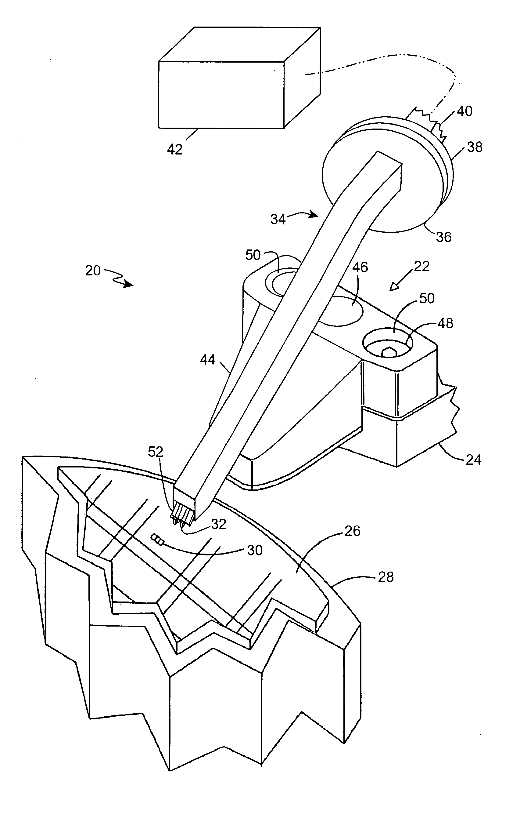
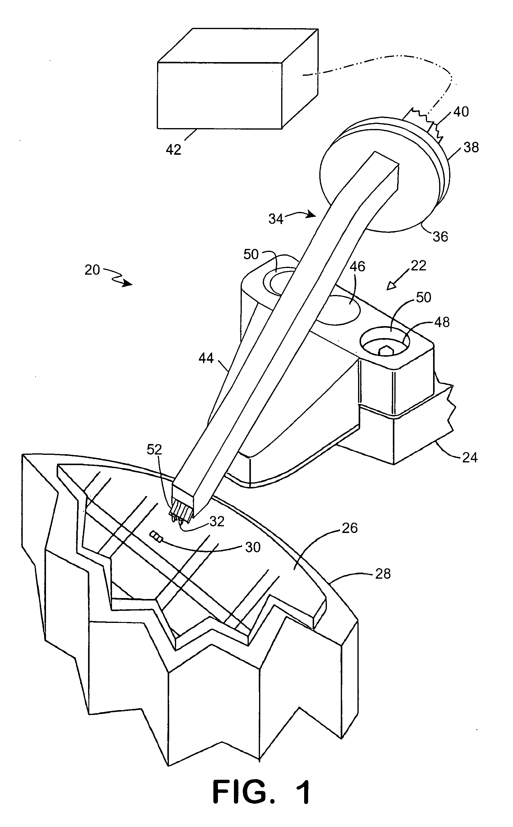
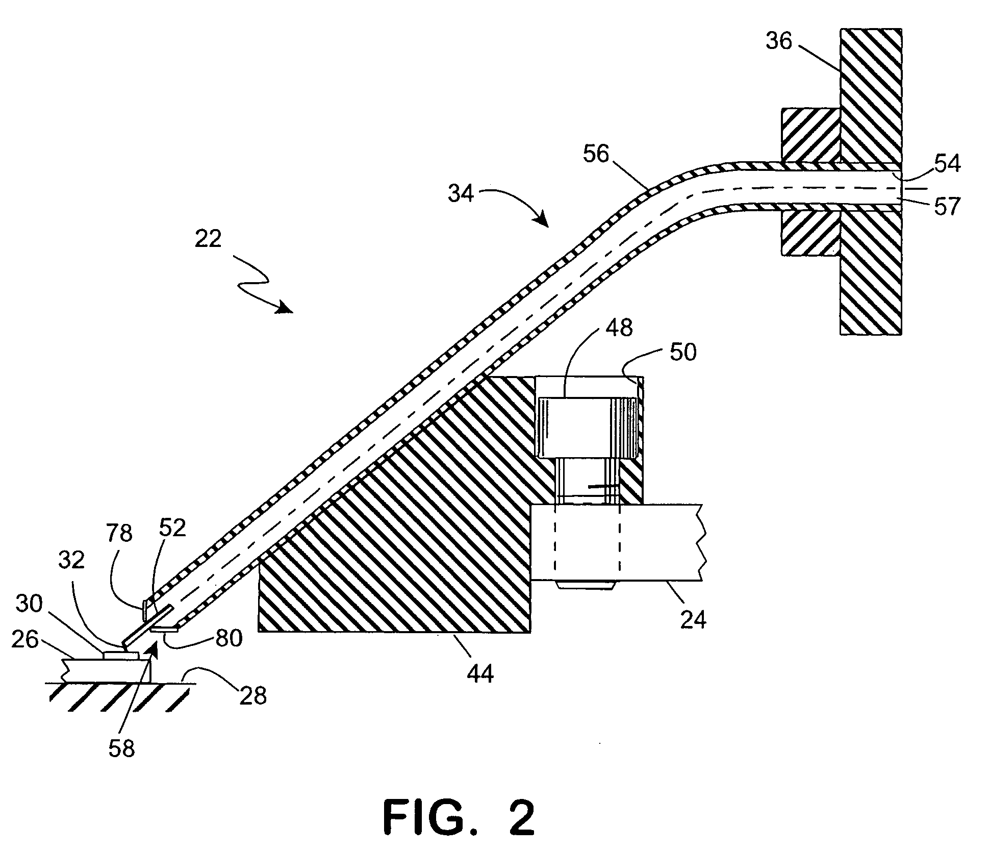
[0024]Integrated circuits (ICs) and other microelectronic devices are fabricated by successively depositing and etching layers of conductive, semi-conductive or insulating material on the surface of a wafer or substrate of semi-conducting material. Typically, the rear surface of the wafer, the back plane, is connected to a ground potential and signals are input to and output by the circuit through conductors that are deposited proximate the front surface of the wafer.

[0025]ICs are commonly inspected “on wafer” by measuring the response of one or more test structures when the structures are stimulated by a test signal. A test structure typically comprises a simple circuit or device under test (DUT) comprising one or more of the elements of the marketable integrated circuits. The devices of the DUT are typically fabricated with the same processes and in the same layers of the wafer fabrication as the corresponding element(s) of the integrated circuit. In addition, a test structure typ...


PUM


Abstract

A wafer probe comprises a contact conductively interconnected with the wall of a waveguide channel and supported by a substrate that projects from an end of a waveguide channel.

Description

CROSS-REFERENCE TO RELATED APPLICATIONS[0001]This application claims the benefit of U.S. Provisional App. No. 60 / 964,103, filed Aug. 8, 2007.BACKGROUND OF THE INVENTION[0002]The present invention relates to a wafer probe for high frequency testing of integrated circuits and other electronic devices.[0003]Integrated circuits (ICs) are economically attractive because large numbers of often complex circuits, for example microprocessors, can be inexpensively fabricated on the surface of a wafer or substrate. Following fabrication, individual dies, including one or more circuits, are separated or singulated and encased in a package that provides for electrical connections between the exterior of the package and the circuit on the enclosed die. The separation and packaging of a die comprises a significant portion of the cost of manufacturing a microelectronic device. To monitor and control the IC fabrication process and to avoid the cost of packaging defective dies, manufacturers commonly...

Claims


Application Information

Patent Timeline
Patent Type & Authority Patents(United States)
IPC IPC(8): G01R31/02H01P1/00
CPCG01R1/06772
Inventor CAMPBELL, RICHARD L.ANDREWS, MICHAEL
Owner CASCADE MICROTECH
Why Eureka
Try Eureka