Optical element and manufacturing method thereof

a manufacturing method and technology of optical elements, applied in the field of optical elements, can solve the problems of increasing the cost, unable to obtain sufficient difference between the core layer and the clad layer for refractive index, and the accuracy of the obtained core diameter, etc., and achieves the effect of low cost and simple and convenient method

Inactive Publication Date: 2005-08-16
FUJIFILM BUSINESS INNOVATION CORP
View PDF13 Cites 14 Cited by
  • Summary
  • Abstract
  • Description
  • Claims
  • Application Information

AI Technical Summary

Benefits of technology

[0024]This invention has been achieved in view of the foregoing problems and intends to provide an optical element having flexibility which is useful for optical wiring. This invent

Problems solved by technology

However, the selective polymerization method (1) involves a problem in bonding the film, the method (2) or (3) increases the cost because of the use of photolithography, and the method (4) has a problem in the accuracy of the diameter for the obtained core.
Further, the method (5) has a problem in that no sufficient difference for the refractive index can be obtained between the core layer and the clad layer.
Then, none of the methods (1) to (5) is suitable to the formation of the polymeric waveguide channel to a large-area, flexible plastic substrate.
However, since the polymer precursor material is thinly filled and cured not only in the capillary grooves but also between the pattern substrate and the planar substrate entirely to form a thin layer of a composition identical with the core layer, it involves a problem that light leaks through the thin layer.
However, since the method uses the monomer as the core forming material, it involves a problem that the volumic shrinkage is large when the monomer is polymerized into a polymer to increase the transmission loss of the polymeric optical waveguide channel.
Further, this is a complicated method of securing the patterned substrate and the planar substrate by clamping, or further seating the contact portion with a resin, so that it is not suitable for mass production and, as a result, the reduction of the cost cannot be expected.
Further, this method cannot be applied to the manufacture of a polymeric optical waveguide channel that uses a film in the thickness of mm order or 1 mm or less as the clad.
However, even when the manufacturing method described in the patent is applied to the manufacture of the polymeric optical waveguide channel, since the cross sectional area of the core portion in the optical waveguide channel is small, it takes much time for forming the core portion and is not suitable for mass production.
Further, it has a drawback that the monomer solution causes a volumic

Method used


Image

  • Optical element and manufacturing method thereof
  • Optical element and manufacturing method thereof
  • Optical element and manufacturing method thereof

Examples


example 1

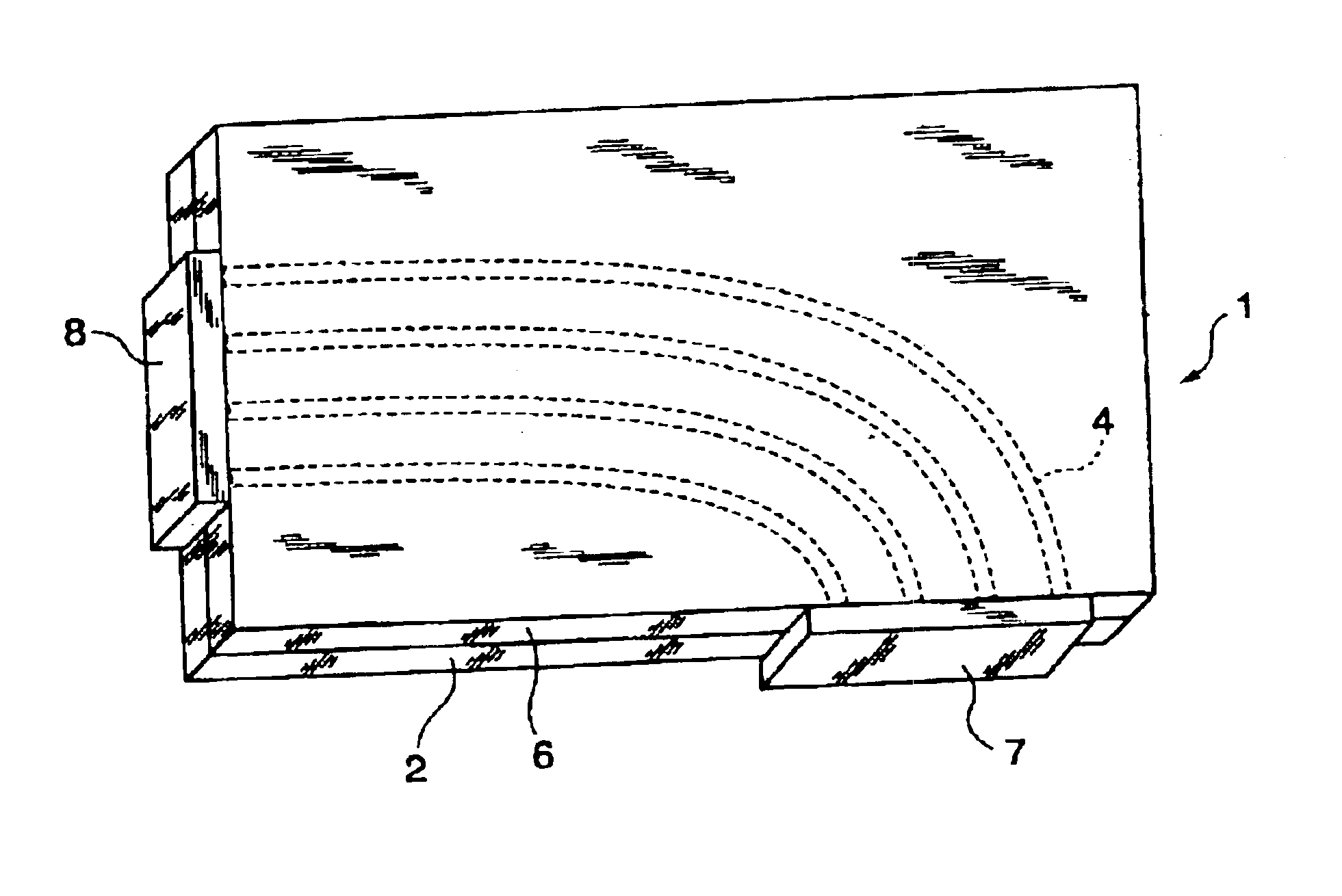
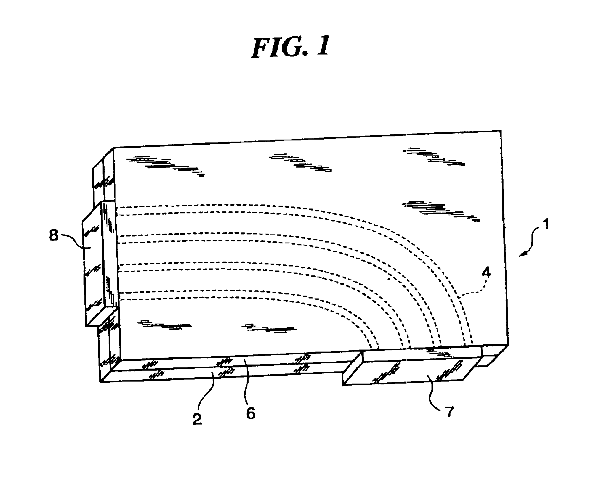
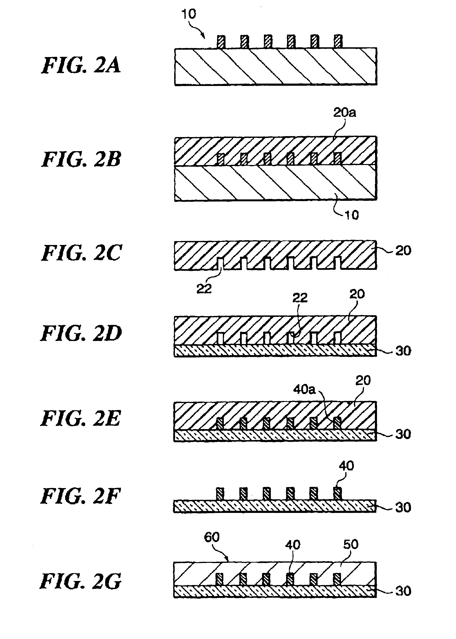
[0091]After coating a thick film resist (SU-8, manufactured by Microchemical Co.) to an Si substrate by a spin coating method, it was prebaked at 80° C., exposed through a photomask and developed to form four convexes each of a square cross section (width: 50 μm, height: 50 μm) as shown in FIG. 1. The distance between each of the convexes was set to 250 μm. Then, it was postbaked at 120° C. to prepare an original substrate for manufacturing an optical waveguide channel core.

[0092]Then, after coating a releasing agent to the original substrate, a thermosetting dimethyl siloxane resin (SYLGARD 184, manufactured by Dow Corning Asia Co.) was cast and cured by heating at 120° C. for 30 minutes and then peeled to prepare a mold having concaves corresponding to the convexes of the square cross section (mold thickness: 3 mm). Further, both ends of the mold were cut to prepare an input / output portion for the following UV-ray curable resin to form a template.

[0093]The template and a film subs...

example 2

[0096]An original substrate for preparing an optical waveguide channel having four convexes each of a square cross section (width: 50 μm, height: 50 μm) was by the same method as in Example 1. Then, after preparing a mold in the same manner as in Example 1, both ends were cut to form a template. The template and an ARTON film (thickness: 180 μm) slightly larger than the template were closely adhered and, when several drops of a thermosetting resin at a viscosity of 500 mPa·s (manufactured by JSR Co.) were dripped to the input / output portion at one end of the template, the concaves were fill with the thermosetting resin by the capillary phenomenon. It was thermally cured by heating for 30 minutes in an oven at 130° C. When the template was peeled from the ARTON film, a core of the same shape as the original substrate convexes was formed on the ARTON film. The refractive index of the core was 1.570. Further, after coating, a thermosetting resin with the refractive index after curing b...

example 3

[0098]An original substrate for preparing an optical waveguide channel having for convexes each of a square cross section (width: 50 μm, height: 50 μm) by the same method as in Example 1. Then, after preparing a mold in the same manner as in Example 1, both ends were cut to form a template. The template and an ARTON film (thickness: 180 μm) slightly larger than the template were closely adhered and several drops of a thermosetting resin at a viscosity of 1300 mPa·s (PJ3001, manufactured by JSR Co.) were dripped to the input / output portion at one end of the template. The template and ARTON film were adhered closely, which were placed in a container depressurized by a vacuum pump (1.0 Pa). The UV-ray curable resin was filled into the concaves instantly by the capillary phenomenon. After taking out the same from the container, the upper portion of the template was irradiated with UV-light at 50 mW / cm2 for 5 minutes to conduct curing and the template was peeled. A core with a refractive...


PUM


Abstract

A flexible optical element useful for optical wiring is provided, in which a light emitting portion is disposed to a core end face of a flexible polymeric optical waveguide channel sheet having a film substrate clad, a core and a clad layer covering the core. A method which enables of manufacturing the optical element in a simple and convenient manner at a low cost is also provided.

Description

BACKGROUND OF THE INVENTION[0001]1. Field of the Invention[0002]This invention relates to an optical element in which a light emitting portion is disposed to a flexible polymeric optical waveguide channel and a manufacturing method thereof.[0003]2. Description of the Related Art[0004]Methods of manufacturing polymeric waveguide channels proposed so far include, for example, (1) a method of impregnating a film with a monomer, selectively exposing a core portion to change the refractive index and bonding the film (selective polymerization method), (2) a method of coating a core layer and a clad layer and then forming a clad portion by use of a reactive ion etching (RIE method), (3) a method of using photolithography of conducting exposure and development by use of a UV-ray curable resin including a polymeric material with a light sensitive material added therein (direct exposure method), (4) a method of utilizing injection molding, and (5) a method of coating a core layer and a clad l...

Claims


Application Information

Patent Timeline
IPC IPC(8): G02B6/13G02B6/43G02B6/138G02B6/42G02B6/122
CPCG02B6/138G02B6/43G02B6/4249
Inventor OHTSU, SHIGEMISHIMIZU, KEISHIYATSUDA, KAZUTOSHIAKUTSU, EIICHI
Owner FUJIFILM BUSINESS INNOVATION CORP
Why Eureka
Try Eureka