Test pattern evaluation method and test pattern evaluation device

a test pattern and evaluation method technology, applied in the direction of individual semiconductor device testing, instrumentation, program control, etc., can solve the problems of spice simulation not being completed in a realistic time, considerable simulation time, and enormous simulation time, so as to reduce simulation time, short simulation time, and high accuracy

Inactive Publication Date: 2011-02-01
SHARP KK
View PDF7 Cites 5 Cited by
  • Summary
  • Abstract
  • Description
  • Claims
  • Application Information

AI Technical Summary

Benefits of technology

The present invention was made in view of the above problems and an object of the present invention is to provide an evaluation method of a test pattern, the method being capable of reducing a simulation time and acquiring a transistor activation rate appropriately with high accuracy, by using a gate-level simulation having a relatively short simulation time as compared with a SPICE simulation.
In addition, in the transistor-level simulation performed by the cell whose circuit scale is very small, since the simulation time is very short and the function number of the cell is limited, the simulation number can be small. Therefore, according to the evaluation method of the test pattern having the seventh characteristic, when the correspondence data is acquired, the transistor-level simulation such as the SPICE simulation can be used. In this case, since the transistor-level simulation is used, the correspondence relation between the cell state and the voltage between the terminals of the transistor can be acquired with higher accuracy. Furthermore, since the transistor-level simulation is not executed for the whole semiconductor integrated circuit in the operation verification, a time required for evaluating the reliability testing test pattern can be prevented from being increased.

Problems solved by technology

However, according to the evaluation technique of the test pattern disclosed in the patent document 1, since the voltage characteristics are analyzed at the transistor level by the SPICE simulation, the simulation time is considerably long.
Especially, when transient analysis of the SPICE is used to perform the simulation with high accuracy, the simulation time is enormously long and the problem is that the SPICE simulation cannot be completed in a realistic time.
Furthermore, as the semiconductor integrated circuit becomes large recently, the SPICE simulation time is increased accordingly, so that it becomes difficult to evaluate the reliability testing test pattern using the SPICE simulation like the evaluation technique of the test pattern disclosed in the patent document 1.
That is, even when the test pattern has a high toggle rate, the evaluation of the reliability test for the gate oxide film of the transistor is not always high.
The toggle rate, fault coverage and the like are not always suitable for the evaluation index of the reliability testing test pattern for the gate oxide film of the transistor.

Method used


Image

  • Test pattern evaluation method and test pattern evaluation device
  • Test pattern evaluation method and test pattern evaluation device
  • Test pattern evaluation method and test pattern evaluation device

Examples


first embodiment

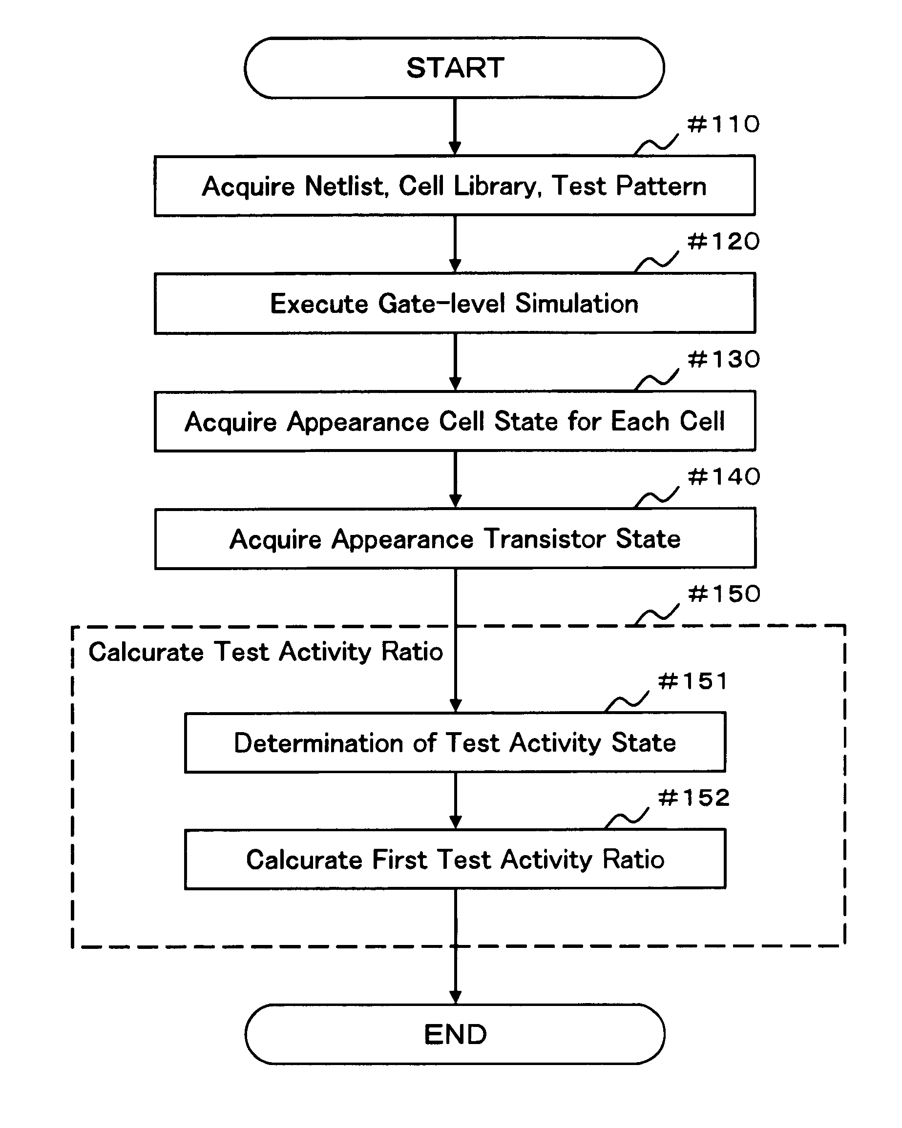
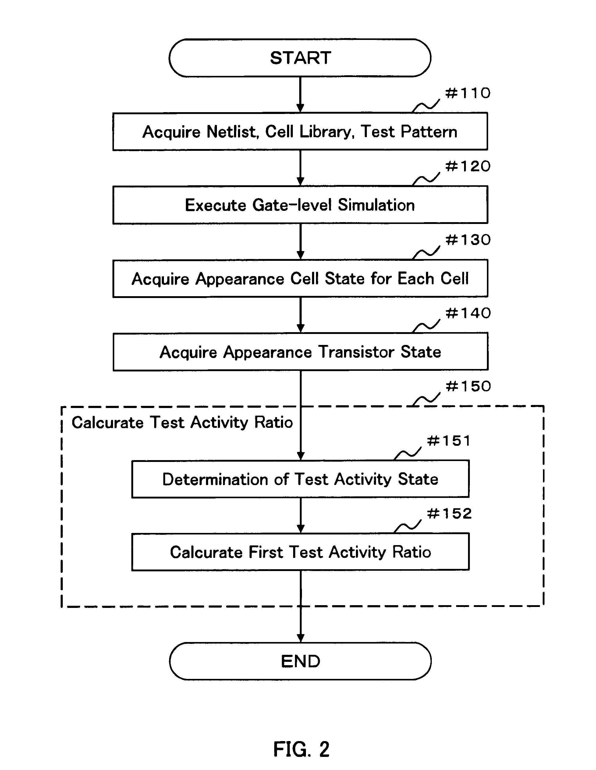
A first embodiment of the method of the present invention and the device of the present invention will be described with reference to FIGS. 1 to 8.

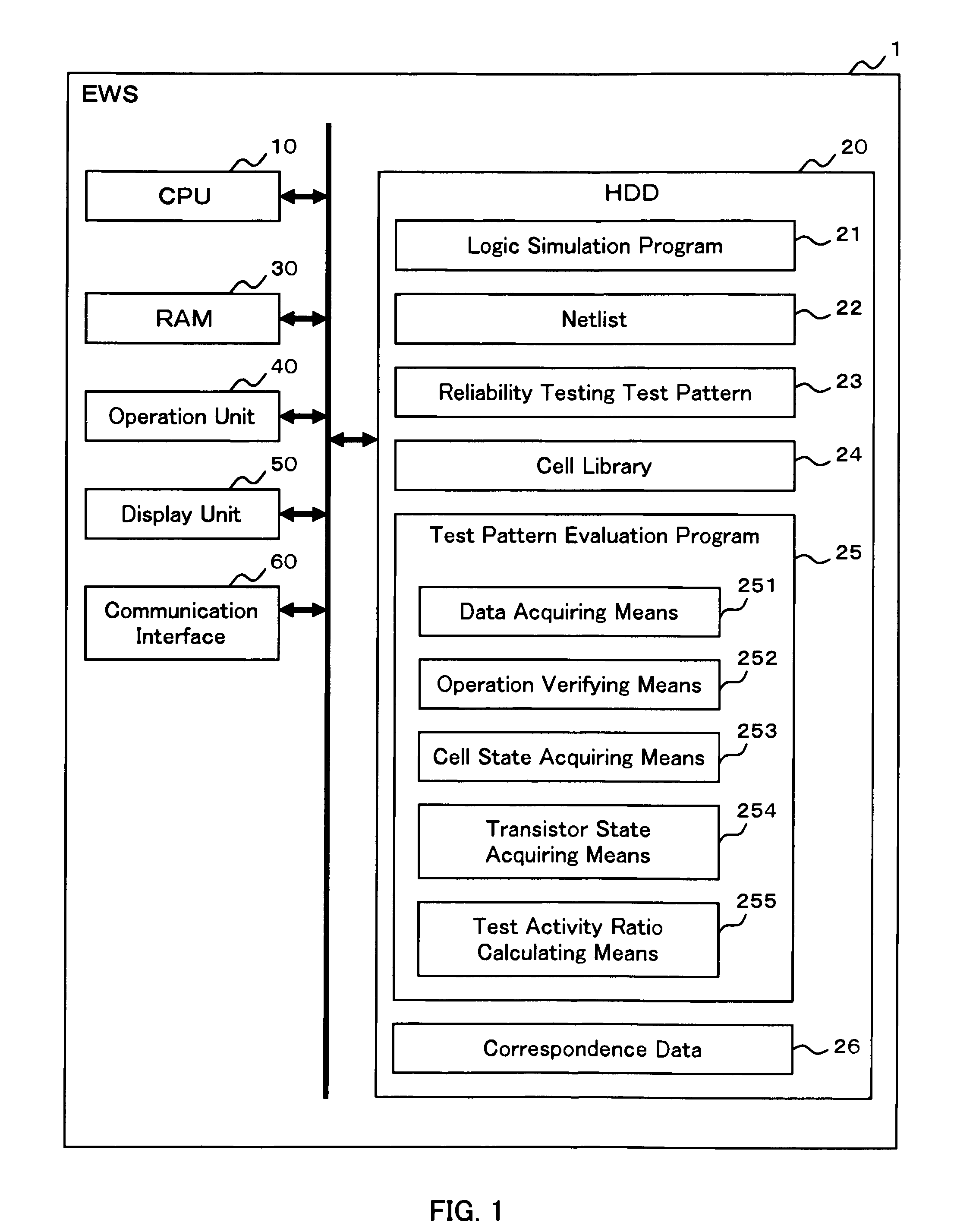
First, a basic constitution of the device of the present invention will be described with reference to FIG. 1. Here, FIG. 1 shows a schematic partial constitution example regarding evaluation of a reliability testing test pattern 23 of an EWS1 (Engineering Workstation) comprising respective means of the device of the present invention.

As shown in FIG. 1, the EWS1 comprises a CPU 10 controlling each function of the EWS1, a HDD 20 storing various kinds of programs and data for implementing each function of the EWS1, a RAM 30 as a temporal memory device comprising a flash memory and the like, an operation unit 40 comprising external input devices such as a keyboard and a mouse, a display unit 50 comprising a device such as a display, and a communication interface 60 communicating data with another device on a LAN.

The HDD 20 in this embodimen...

second embodiment

A second embodiment of the method of the present invention and the device of the present invention will be described with reference to FIG. 9. In addition, in this embodiment, a case where a determination method of the test activity state is different from that of the first embodiment will be described.

A method of the present invention according to this embodiment will be described with reference to FIGS. 2 and 9 hereinafter.

Similarly to the first embodiment, data acquiring means 251 in a device in this embodiment of the present invention acquires a gate-level netlist 22 of a semiconductor integrated circuit to be verified, a reliability testing test pattern 23, a cell library 24 from a HDD 20 (step #110), and operation verifying means 252 starts a logic simulation program 21 and carries out a logic simulation at a gate level (step #120). In addition, the gate-level netlist 22 of the semiconductor integrated circuit, the reliability testing test pattern 23, and the cell library 24 i...

third embodiment

A third embodiment of the method of the present invention and the device of the present invention will be described with reference to FIG. 10. In addition, in this embodiment, a description will be made of a case where the contents of the test activity ratio are different from those of the first and second embodiments. More specifically, in the above first and second embodiments, the ratio of the transistors in the test activity state to the whole transistors in the semiconductor integrated circuit is calculated as a first test activity ratio whereas, in this embodiment, a second test activity ratio is calculated by adding up the ratios of the appearance transistor state to all the transistor states, for all the transistors in the semiconductor integrated circuit.

The method of the present invention in this embodiment will be described with reference to FIG. 10 hereinafter. Here, FIG. 10 shows a process procedure of the method of the present invention in this embodiment.

Similarly to ...


PUM


Abstract

Provided are an evaluation method and device of a test pattern which enable an appropriate evaluation in a reliability test with a simulation time reduced and high accuracy. It is assumed that each possible internal state of a cell determined at least by a logic value or a voltage value of an input terminal is a cell state, and each possible state of a transistor determined by a voltage between terminals of the transistor is a transistor state. The method comprises steps of: verifying operation of a semiconductor integrated circuit at a gate level or higher; acquiring an appearance cell state continuously appearing for a predetermined time or more in the operation verification; acquiring an appearance transistor state using the corresponding appearance cell state in the operation verification for each transistor; and calculating a test activity ratio of the transistor using the corresponding appearance transistor state for each transistor.

Description

CROSS REFERENCE TO RELATED APPLICATIONThis Nonprovisional application claims priority under 35 U.S.C. §119(a) on Patent Application No. 2007-261333 filed in Japan on Oct. 4, 2007, the entire contents of which are hereby incorporated by reference.BACKGROUND OF THE INVENTION1. Field of the InventionThe present invention relates to a test pattern evaluation method and a test pattern evaluation device for a reliability test of a semiconductor integrated circuit.2. Description of the Related ArtConventionally, in order to ship a highly reliable semiconductor integrated circuit device, various kinds of reliability tests are performed for the semiconductor integrated circuit device before shipment. The reliability tests include an endurance test for a gate oxide film of a transistor constituting a semiconductor integrated circuit. More specifically, in the endurance test for the gate oxide film of the transistor, while an endurance testing power supply voltage higher than a rated voltage i...

Claims


Application Information

Patent Timeline
Patent Type & Authority Patents(United States)
IPC IPC(8): G06F17/50
CPCG06F17/5022G01R31/31835G06F30/33
Inventor KUCHII, TOSHIMASA
Owner SHARP KK
Why Eureka
Try Eureka