Semiconductor memory device and method of fabrication of the same

a memory device and semiconductor technology, applied in the direction of semiconductor devices, transistors, electrical devices, etc., can solve the problems of increasing memory capacity increasing coupling noise between floating gates, etc., to reduce the value of coupling noise and reduce the coupling noise between floating electrodes neighboring in the word line direction

Inactive Publication Date: 2011-02-08
KK TOSHIBA
View PDF10 Cites 7 Cited by
  • Summary
  • Abstract
  • Description
  • Claims
  • Application Information

AI Technical Summary

Benefits of technology

[0098]According to the semiconductor memory device and the fabrication method relating to the present embodiment, at least the following advantageous effects (1) and (2) can be obtained.
[0099](1) Microfabrication can advantageously be achieved, and the coupling noise between the floating electrodes neighboring in the word line direction can be reduced.
[0100]As described above, the first and second memory cell transistors MT1 and MT2 according to the present embodiment include the L-shaped floating electrode FG comprising the first floating electrode FG1 provided on the tunnel insulation film 19, and the second floating electrode FG2 provided on one end portion of the first floating electrode FG1.
[0101]The distance d2 between the second floating electrodes FG2, which neighbor in the word line direction, of the first and second memory cell transistors MT1 and MT2 is greater than the distance d1 between the first floating electrodes FG1 which neighbor in the word line direction (distance: d2>d1).
[0102]Since the distance d2 is greater than the distance d1, as described above, even if the distance d1 between the first floating electrodes FG1 is less than about double the thickness of the inter-gate insulation film IPD, the space between the neighboring floating electrodes FG is not entirely filled with the inter-gate insulation film IPD. Therefore, the control electrode CG (word line WL) can be formed on the inter-gate insulation film IPD that is present between the second floating electrodes FG2.
[0103]A fixed voltage of, e.g. 0V can be applied to the control electrode CG. Thus, since the parasitic capacitance C0 between the first floating electrodes FG1 can be reduced, the coupling noise between the floating electrodes FG can be shielded and the value of the coupling noise can be reduced.

Problems solved by technology

Under the circumstances, in addition to the enhancement in functions, the increase in memory capacity is a challenge to the NAND flash memory.
However, if the microfabrication of memory cells is advanced, the parasitic capacitance between floating gates (FG), which neighbor in a word line direction (i.e. the direction of wiring of control gates (CG)), increases, and consequently the coupling noise between the floating gates (FG) increases.
Consequently, since the parasitic capacitance between the floating gates (FG) increases, the coupling noise between the floating gates (FG) increases.

Method used


Image

  • Semiconductor memory device and method of fabrication of the same
  • Semiconductor memory device and method of fabrication of the same
  • Semiconductor memory device and method of fabrication of the same

Examples


first embodiment

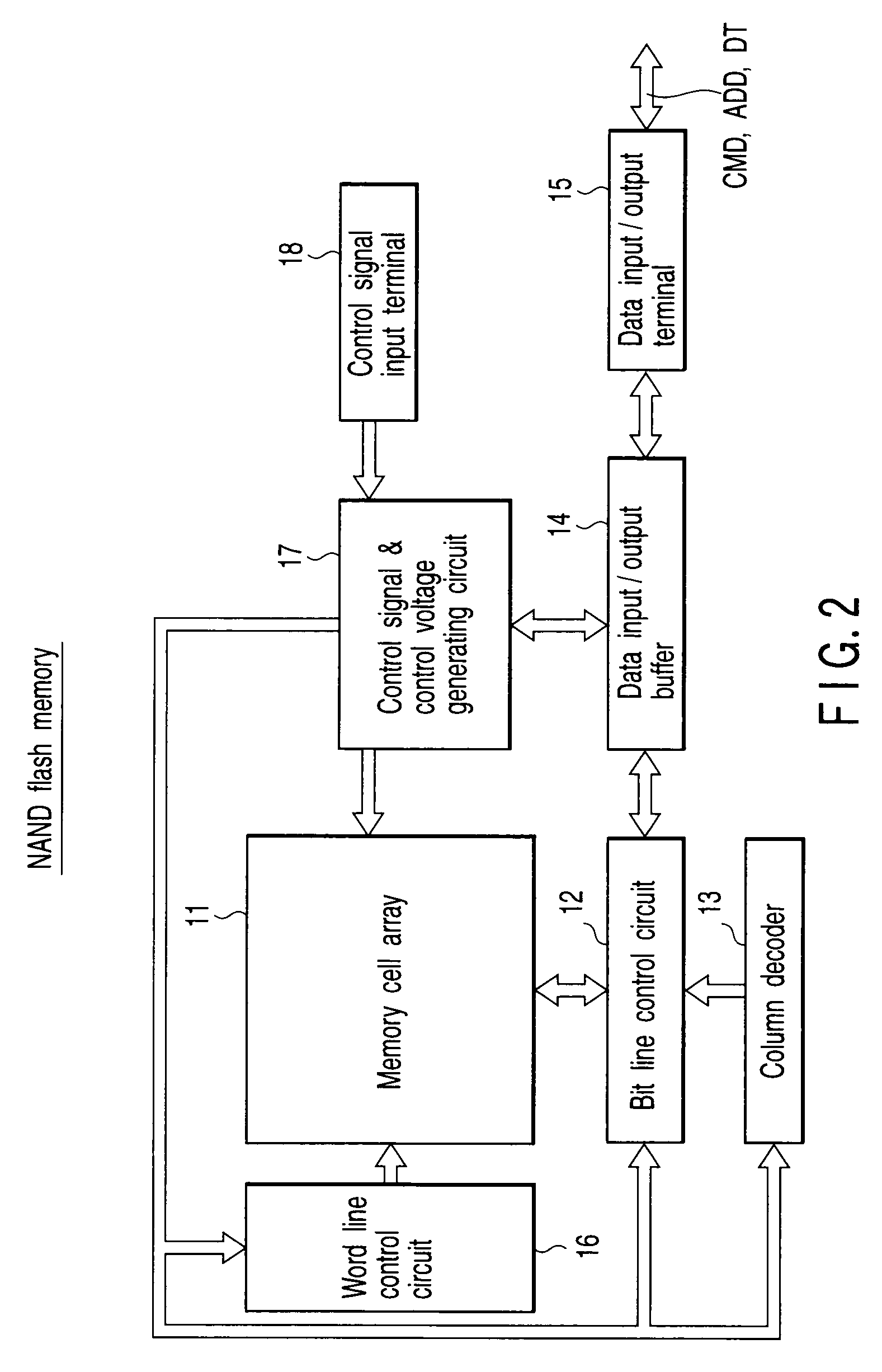
[0055]To begin with, referring to FIG. 2, a description is given of the entire structure of a semiconductor memory device according to a first embodiment of the present invention. FIG. 2 is a block diagram showing a NAND flash memory according to this embodiment.

[0056]As shown in FIG. 2, the NAND flash memory comprises a memory cell array 11, a bit line control circuit 12, a column decoder 13, a data input / output buffer 14, a data input / output terminal 15, a word line control circuit 16, a control signal & control voltage generating circuit 17, and a control signal input terminal 18.

[0057]The memory cell array 11 is composed of a plurality of blocks. The word line control circuit 16 for controlling word lines and the bit line control circuit 12 for controlling bit liens are connected to the memory cell array 11.

[0058]The bit line control circuit 12 reads data of memory cell transistors in the memory cell array 11 via the bit lines, and detects the states of the memory cell transisto...

modification 1 (

[Modification 1 (Another Example of Fabrication Method)]

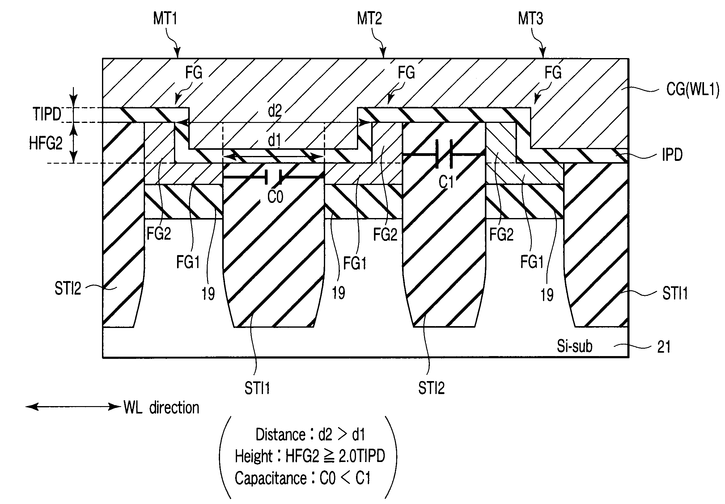
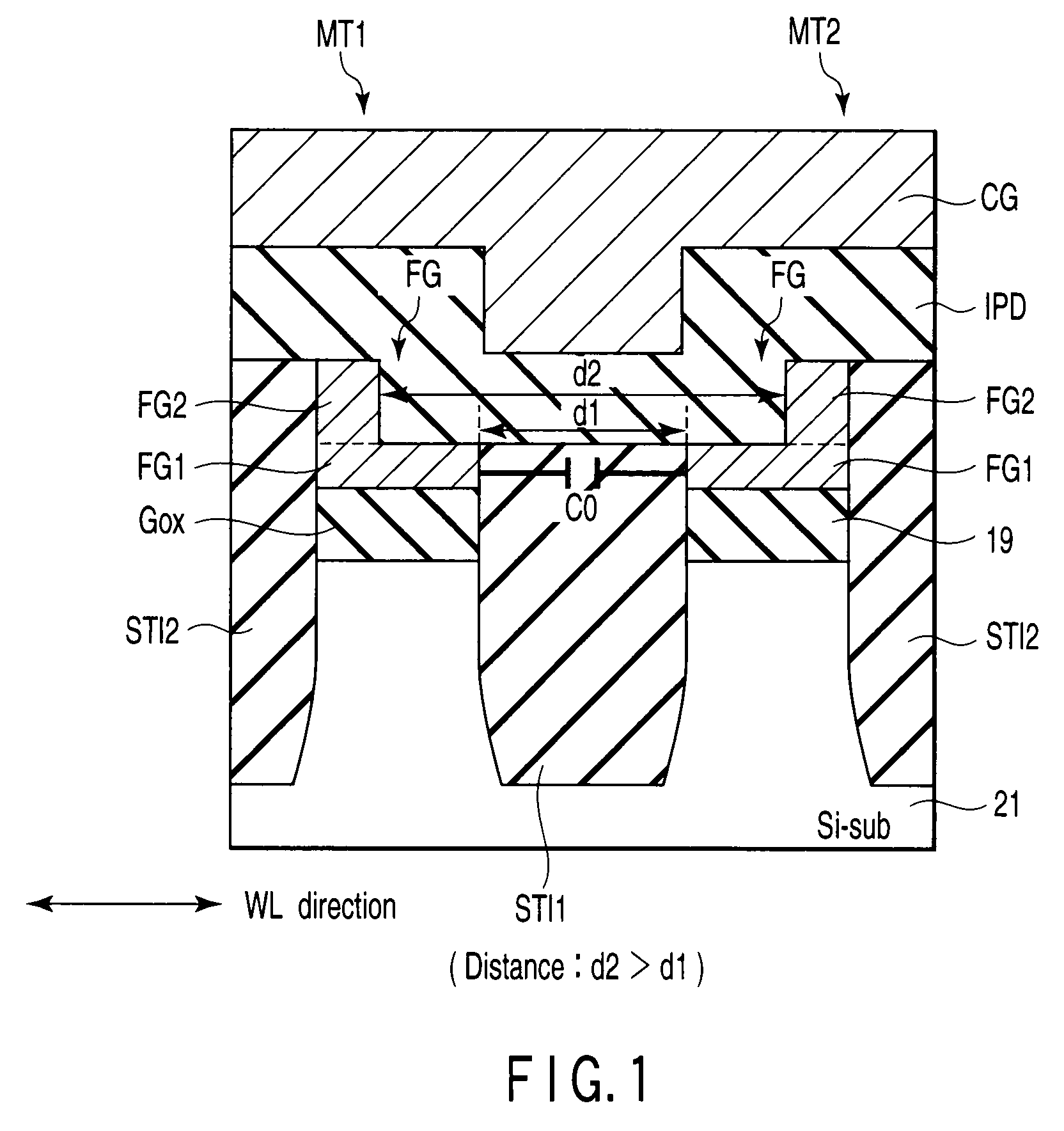
[0110]Next, a method of fabrication of the semiconductor memory device according Modification 1 is described with reference to FIG. 12 to FIG. 17. Modification 1 relates to another example of the fabrication method of the semiconductor memory device which has been described in connection with the first embodiment. A detailed description of the parts common to those in the first embodiment is omitted. In the description below, the memory cell transistor MT1, MT2, which has been described with reference to FIG. 4, is exemplified.

[0111]To start with, as shown in FIG. 12, using the same fabrication steps as in the first embodiment, a tunnel insulation film 19, a floating electrode material 41 and a first mask material 43 are successively formed on the semiconductor substrate 21.

[0112]As shown in FIG. 13, a photoresist 45 is coated on the first mask material 43. The photoresist 45 is exposed and developed, and the photoresist 45 is ...

second embodiment

Modification of Second Embodiment

[0136]A semiconductor memory device according to a modification of the second embodiment of the invention is described with reference to FIG. 21. According to this modification, an air gap 77 is provided in the central part of the low dielectric film 55 of the second embodiment. In the description below, a detailed description of the parts common to those in the second embodiment is omitted.

[0137]As shown in FIG. 21, memory cell transistors MT1, MT2 and MT3 according to the modification are featured in that an air gap 77 is provided in the central part of the low dielectric film 55 of a second device isolation insulation film STI2. The air gap is vacuum or filled with an inert gas such as nitrogen gas or with air. This means that the air gap 77 has a lower dielectric constant ∈3 than the dielectric constant of the low dielectric constant film 55.

[0138]In addition to the advantageous effects of the second embodiment, the modification provides the adva...


PUM


Abstract

A semiconductor memory device includes a first memory cell transistor. The first memory cell transistor includes a tunnel insulation film provided on a semiconductor substrate, a floating electrode provided on the tunnel insulation film, an inter-gate insulation film provided on the floating electrode, and a control electrode provided on the inter-gate insulation film. The floating electrode includes a first floating electrode provided on the tunnel insulation film and a second floating electrode provided on one end portion of the first floating electrode, the floating electrode having an L-shaped cross section in a wiring direction of the control electrode.

Description

CROSS-REFERENCE TO RELATED APPLICATIONS[0001]This application is based upon and claims the benefit of priority from prior Japanese Patent Application No. 2007-050118, filed Feb. 28, 2007, the entire contents of which are incorporated herein by reference.BACKGROUND OF THE INVENTION[0002]1. Field of the Invention[0003]The present invention relates to a semiconductor memory device and a method of fabricating the semiconductor memory device, and this invention is applied, for example, to a NAND flash memory.[0004]2. Description of the Related Art[0005]In recent years, semiconductor memory devices, for example, NAND flash memories, have begun to be used as main memories of various electronic devices, such as portable audio devices, by virtue of their merits of large capacity and nonvolatility.[0006]Under the circumstances, in addition to the enhancement in functions, the increase in memory capacity is a challenge to the NAND flash memory. The simplest method for realizing the increase in...

Claims


Application Information

Patent Timeline
Patent Type & Authority Patents(United States)
IPC IPC(8): H01L29/788H01L21/336
CPCH01L21/28273H01L27/115H01L27/11521H01L29/42324H01L29/7881H01L29/40114H10B69/00H10B41/30H10B41/35H01L21/76205
Inventor WATANABE, TOSHIHARU
Owner KK TOSHIBA
Why Eureka
Try Eureka