Scanning electron microscope and method of imaging an object by using the scanning electron microscope

a scanning electron microscope and scanning electron technology, applied in material analysis using wave/particle radiation, instruments, nuclear engineering, etc., can solve the problems of long time taken to perform switching operations, deterioration of reproducibility, and varied magnetic field, and achieve high reproducibility, high resolution, and high speed

Inactive Publication Date: 2011-02-15
HITACHI HIGH-TECH CORP
View PDF7 Cites 10 Cited by
  • Summary
  • Abstract
  • Description
  • Claims
  • Application Information

AI Technical Summary

Benefits of technology

[0007]It is a first object of the present invention to provide a technique for moving the focal point of a condenser lens at high speed in cases where the movement is made such that a low-magnification image is obtained with a large depth of focus and that a high-magnification image is obtained with high resolution.
[0008]It is a second object of the invention to provide a technique of enhancing the reproducibility of movement of the focal point of a condenser lens in cases where the movement is made such that a low-magnification image is obtained with a large depth of focus and that a high-magnification image is obtained with high resolution.
[0010]That is, a scanning electron microscope according to the present invention has: a specimen-holding portion for holding a specimen; an electron beam source emitting an electron beam; a condenser lens for converging the electron beam emitted from the electron beam source; an objective lens for focusing the converged beam into a very small spot onto the specimen; scan coils for scanning the electron beam over the specimen; a detector for detecting a specimen signal emanating from the specimen in response to the electron beam irradiation; and a display portion for displaying the specimen signal detected by the detector as an image. An axisymmetric electrode is mounted within the magnetic field produced by the condenser lens. A voltage is applied to the electrode. Consequently, the image point of the condenser lens is moved with high speed and high reproducibility.
[0011]According to the present invention, movement of the image point of the condenser lens is made to obtain a low-magnification image with a large depth of focus and a high-magnification image is obtained with high resolution. This movement is achieved with high speed and high reproducibility.

Problems solved by technology

If the electrical current flowing through a coil is varied to vary the excitation of the electromagnetic lens, there is the possibility that the magnetic field is varied with delay by magnetic after-effect or the reproducibility is deteriorated by the effects of hysteresis.
Where the aperture angle of the electron beam is switched with an electromagnetic lens, a long time is taken to perform the switching operation.
Consequently, there is the anxiety that the throughput is deteriorated.

Method used


Image

  • Scanning electron microscope and method of imaging an object by using the scanning electron microscope
  • Scanning electron microscope and method of imaging an object by using the scanning electron microscope
  • Scanning electron microscope and method of imaging an object by using the scanning electron microscope

Examples


first embodiment

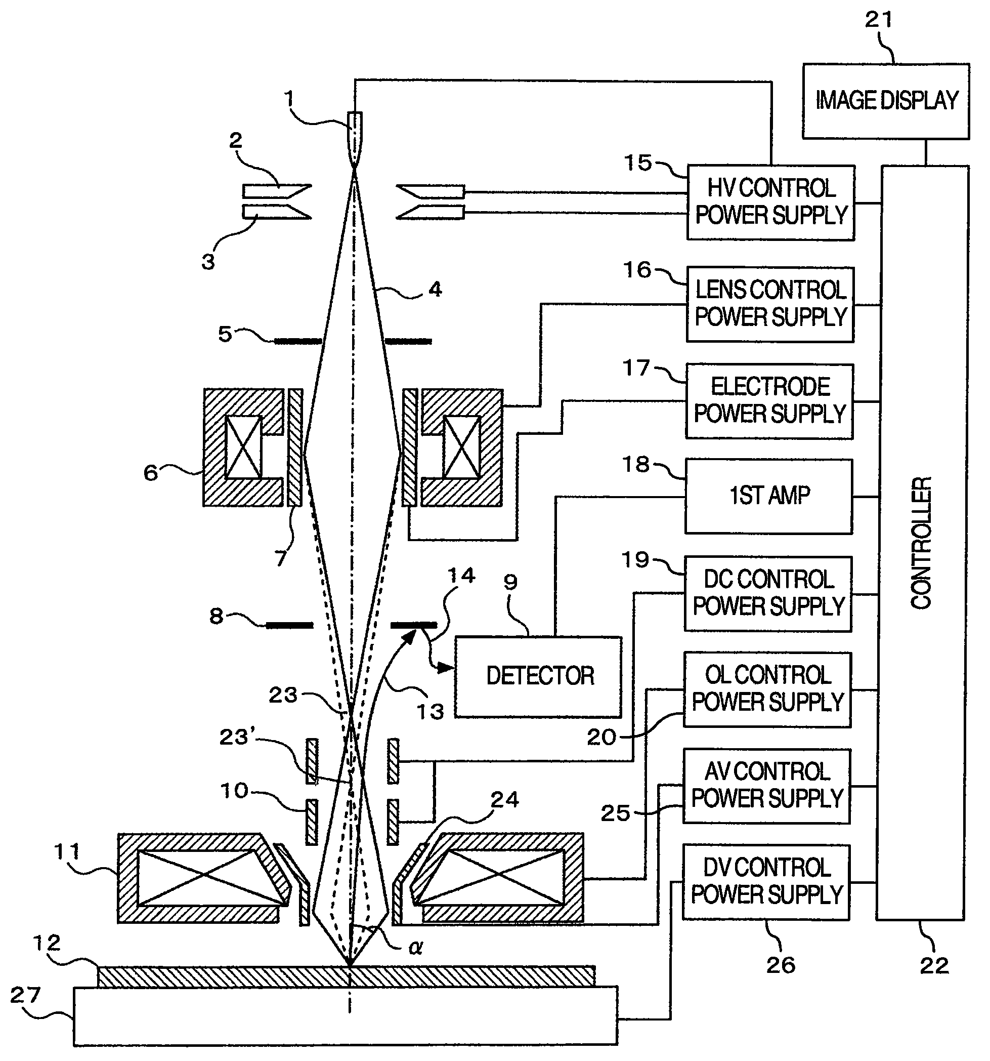
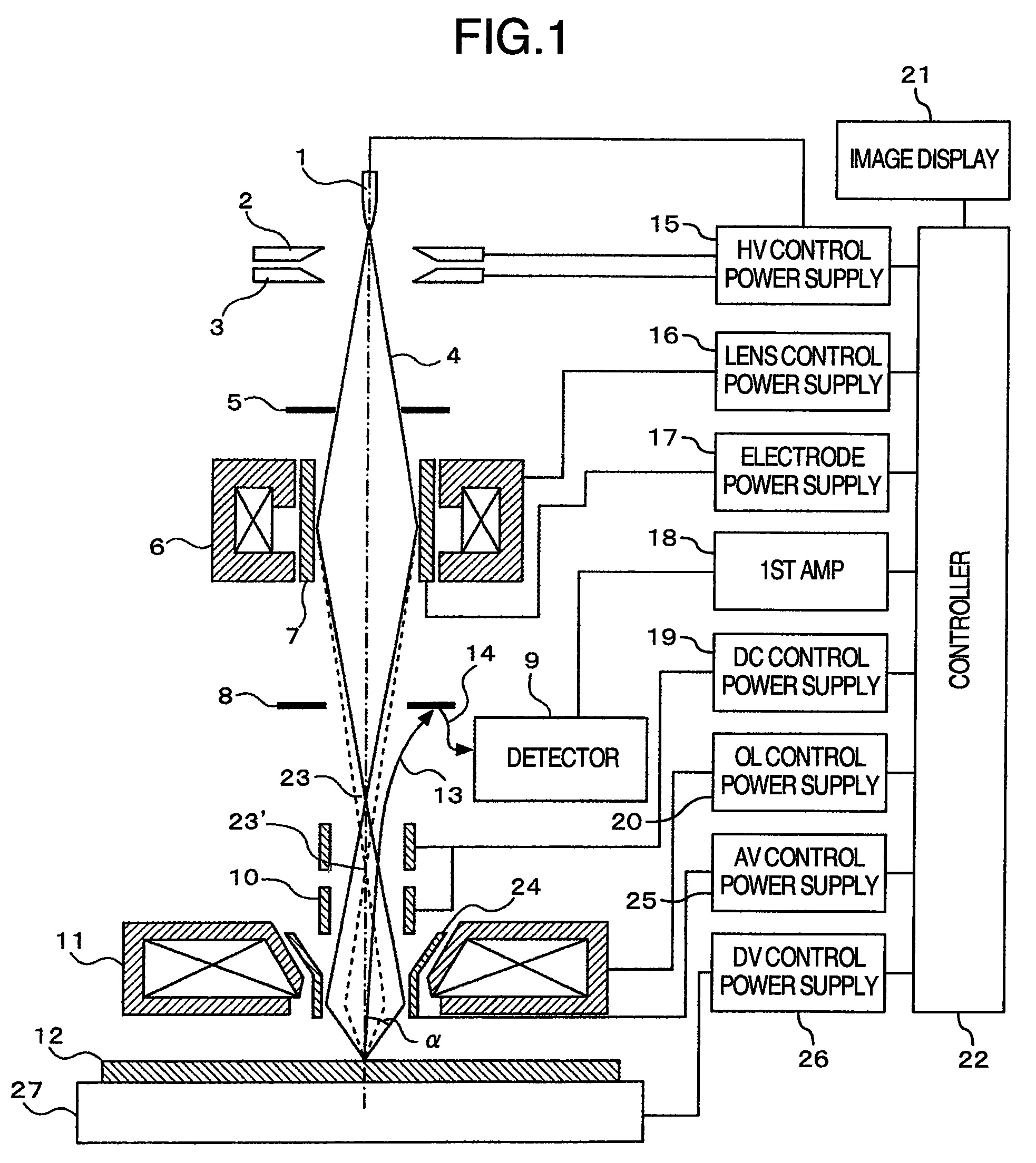
[0019]FIG. 1 is a schematic cross-sectional view showing the structure of a scanning electron microscope according to the present invention. In the figure, a vacuum vessel, a wafer-conveying system, and so on necessary for the scanning electron microscope are omitted. A voltage is applied between a cathode 1 and a first anode 2 from a high-voltage (HV) control power supply 15 that is under control of a controller 22. A given emission current is extracted from the cathode 1. An accelerating voltage is applied between the cathode 1 and a second anode 3 from the high-voltage control power supply 15 that is under control of the controller 22. Therefore, a primary electron beam 4 released from the cathode 1 is accelerated toward a rear stage of lenses. After undesired regions of the primary electron beam 4 are removed by an aperture plate 5, the beam 4 is focused at a focal position 23 by a condenser lens 6 that is under control of a lens control power supply 16.

[0020]Then, the primary e...

second embodiment

[0029]FIG. 3 is a vertical cross section showing the structure of a scanning electron microscope according to the present invention. This structure is similar to the structure already described in connection with FIG. 1 except that the condenser lens 6 of FIG. 1 is replaced by two stages of condenser lenses consisting of a first condenser lens 6a and a second condenser lens 6b that are controlled by lens control power supplies 16a and 16b. respectively. The aperture plate 5 is disposed between the first condenser lens 6a and the second condenser lens 6b to remove regions not necessary for formation of an image from the primary electron beam 4. Then, the beam is converged by the second condenser lens 6b and focused into a very small spot onto the specimen 12 by the objective lens 11 that is under control of the objective lens control power supply 20. The amount of the primary electron beam 4 passed through the aperture plate 5 is adjusted by controlling the focal position 23 of the f...

third embodiment

[0031]FIG. 4 is a vertical cross section showing the structure of a scanning electron microscope according to the present invention. This structure is characterized in that an axisymmetric electrode 7b is disposed within the magnetic field generated by the second condenser lens 6b shown in FIG. 3. The aperture angle α is determined by the focal position 23a of the first condenser lens 6a, the diameter of the aperture in the aperture plate 5, and the focal position 23b of the second condenser lens. When a voltage is applied to the axisymmetric electrode 7a disposed within the magnetic field set up by the first condenser lens 6a from an electrode power supply 17b, the focal position 23a of the first condenser lens 6a varies, thus changing the amount of the primary electron beam 4 impinging on the specimen 12. However, the aperture angle α also varies because the focal position 23a of the first condenser lens 6a varies. Accordingly, the aperture angle α can be controlled by applying a ...


PUM

PropertyMeasurementUnit
scanning electron microscopeaaaaaaaaaa
magnetic fieldaaaaaaaaaa
voltageaaaaaaaaaa

Abstract

A scanning electron microscope capable of modifying the focal position of a condenser lens with high speed and high reproducibility in order that low-magnification images are obtained at large depths of focus and that high-magnification images are obtained at high resolution. The microscope has a specimen-holding portion, an electron beam source, a condenser lens for converging the electron beam, an objective lens for focusing the converged beam into a very small spot onto a specimen, scan coils, a detector for detecting a specimen signal emanating from the specimen, and a display portion for displaying the detected specimen signal as an image. An axisymmetric electrode is disposed within the magnetic field produced by the condenser lens. A voltage is applied to the electrode.

Description

BACKGROUND OF THE INVENTION[0001]The present invention relates to a scanning electron microscope for obtaining a two-dimensional image of a specimen by scanning a focused electron beam over the specimen and detecting the produced secondary signal. Especially, the invention relates to a scanning electron microscope for measuring patterns formed on substrates such as semiconductor substrates and for observing defects.[0002]Semiconductor devices are fabricated by forming a pattern on a photomask, transferring the pattern onto a wafer by lithography and etching steps, and repeating this sequence of operations. In this manufacturing process, it is important to achieve a good yield quickly and to maintain stable operation of the production process. For these purposes, it is essential that in-line inspection of wafers be performed, found defects be quickly analyzed, causes of generation of the defects be sought for, and the sought causes be utilized for countermeasures. To quickly couple t...

Claims


Application Information

Patent Timeline
Patent Type & Authority Patents(United States)
IPC IPC(8): H01J37/28G01N23/225
CPCG01N23/225H01J37/21H01J37/265H01J37/28H01J2237/2817H01J2237/21H01J2237/2611H01J2237/2814
Inventor TACHIBANA, ICHIROSATO, MITSUGUSUZUKI, NAOMASA
Owner HITACHI HIGH-TECH CORP
Why Eureka
Try Eureka