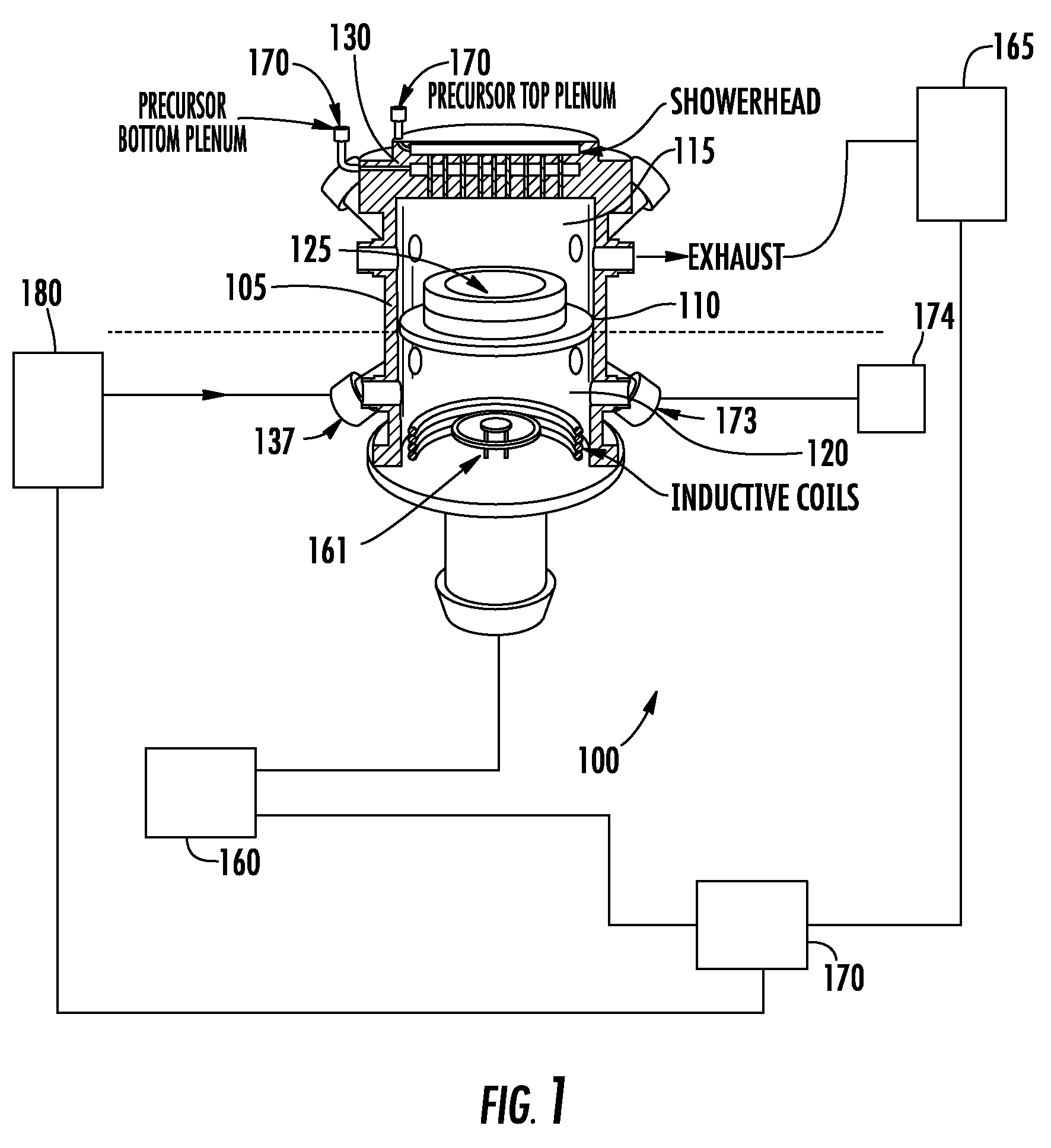
Dual chamber system providing simultaneous etch and deposition on opposing substrate sides for growing low defect density epitaxial layers
a dual chamber and substrate technology, applied in the direction of polycrystalline material growth, crystal growth process, after-treatment details, etc., can solve the problems of difficult direct growth of gan on sic, no readily available suitable substrate material, and difficult to obtain gan bulk crystals. , to achieve the effect of low d
- Summary
- Abstract
- Description
- Claims
- Application Information
AI Technical Summary
Benefits of technology
Problems solved by technology
Method used
Image

Examples
Embodiment Construction
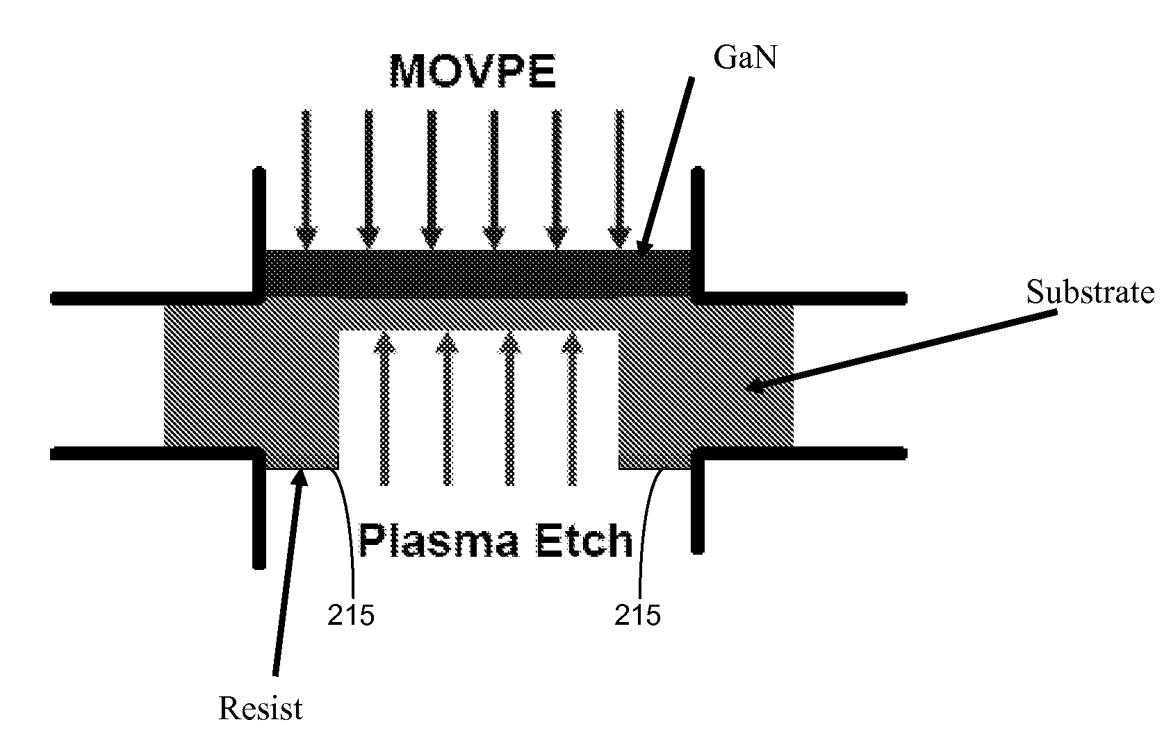
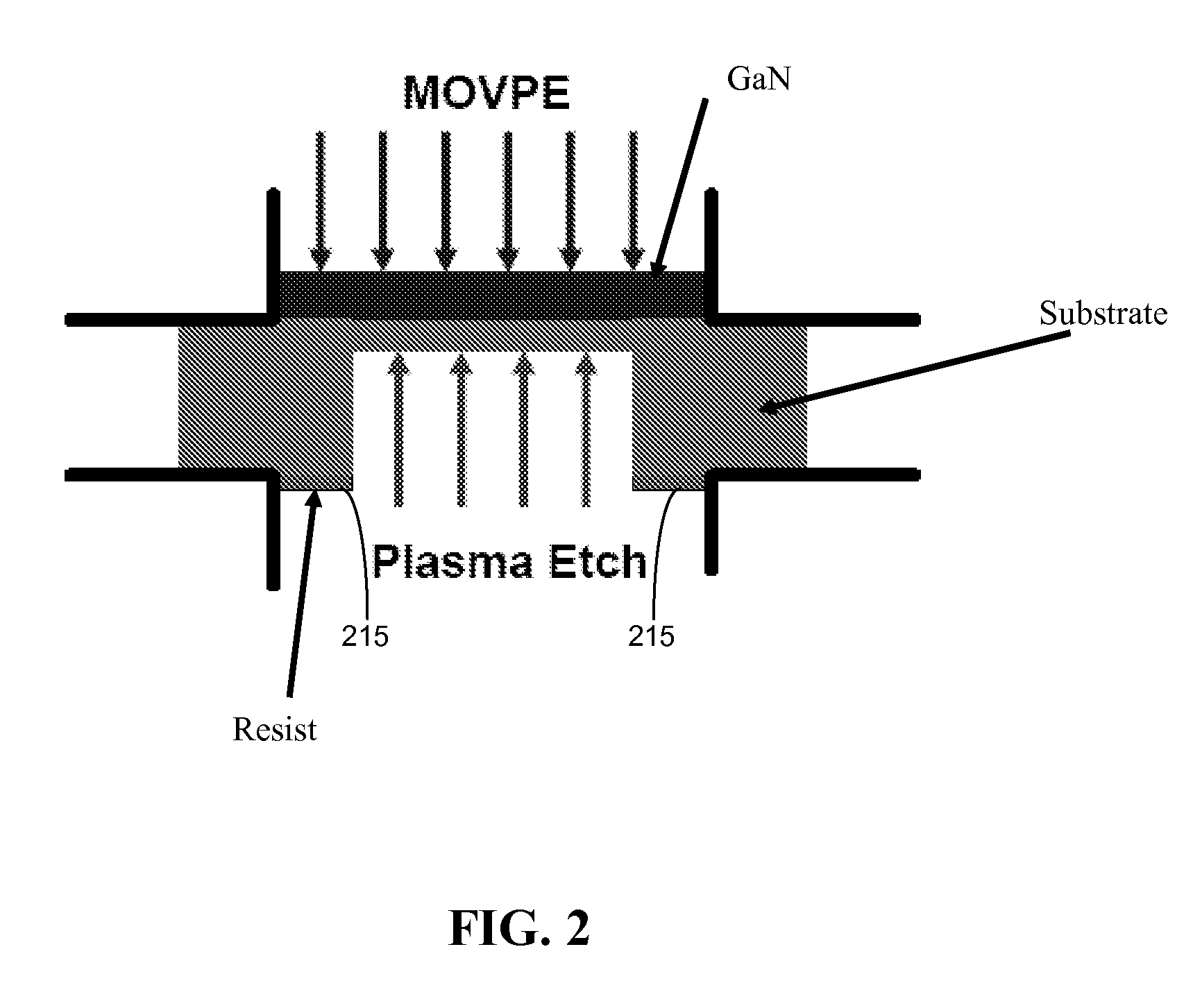
[0018]Thinning of a substrate to maintain critical thickness values during the deposition of an epitaxial film has been found by the present Inventors to reduce lattice mismatch stresses in the film. The substrate can be thinned (e.g., continuously) by etching from the backside so that it accommodates the mismatch strain in the epitaxial film to a greater extent as the film grows thicker and thicker. Lower stresses in the epitaxial film during deposition can result in epitaxial films having a lower defect density. Lower defect density epitaxial films can permit improved device performance, such as for LED devices and power transistors. In a preferred embodiment, the epitaxial film can be grown on thinned substrate regions at the center of the wafer, while at the edges, the substrate can be relatively thick and interfacial stress will be relaxed by misfit dislocations and other defects in the film which are preferentially formed over those regions.
[0019]In one exemplary embodiment, w...
PUM
| Property | Measurement | Unit |
|---|---|---|
| temperatures | aaaaa | aaaaa |
| surface roughness | aaaaa | aaaaa |
| thickness | aaaaa | aaaaa |
Abstract
Description
Claims
Application Information
 - R&D
- Intellectual Property
- Life Sciences
- Materials
- Tech Scout
- Unparalleled Data Quality
- Higher Quality Content
- 60% Fewer Hallucinations
Browse by: Latest US Patents, China's latest patents, Technical Efficacy Thesaurus, Application Domain, Technology Topic, Popular Technical Reports.
© 2025 PatSnap. All rights reserved.Legal|Privacy policy|Modern Slavery Act Transparency Statement|Sitemap|About US| Contact US: help@patsnap.com