Wafer level system in package and fabrication method thereof

a technology of wafer level and package, applied in the field of stack type packages, can solve the problems of increasing processing and fabrication costs, limiting the size of a device corresponding to a fine pitch, and enhancing circuit integration

Active Publication Date: 2011-03-15
NEPES CO LTD
View PDF10 Cites 3 Cited by
  • Summary
  • Abstract
  • Description
  • Claims
  • Application Information

AI Technical Summary

Benefits of technology

[0010]An aspect of the present invention provides an integrated package having a new structure, in which various kinds of electronic devices can be easily integrated.
[0012]Another aspect of the present invention provides an SiP, in which heat can be easily radiated, and signals can be smoothly processed in high-speed operation.
[0022]According to the present invention, since various kinds of devices are buried at a wafer level as compared to a technology for burying devices in a package substrate or printed circuit board, a more integrated semiconductor device can be implemented corresponding to demand for a fine pitch. Further, the heat radiation of devices required in high-speed operation and high heat generation is maximized by virtue of the multi-stepped heat radiation structure, and the operations of the devices are more stabilized. The heat radiation structure can be implemented with a single heat sink, a heat sink connected to heat pipes, or a complex structure including a heat radiation plate, heat pipes and a heat sink.
[0023]Since an infrastructure implemented under a conventional wafer level process can be used in an integrated semiconductor package having such a complex structure, costs for initial equipment investment can be minimized.

Problems solved by technology

However, the SoC, which is configured by stacking various circuits on one single chip, has a technical limit in enhancing circuit integration.
However, since burying and stacking processes are performed on a package substrate or main board in the package by the burying and build-up method, there is a limit in reducing the size of a device corresponding to a fine pitch.
Further, since a redistribution process for electrical connection between embedded chips should be essentially added due to the limit of a fine pitch to be applied, time for processing and fabrication cost are increased.
Furthermore, when a semiconductor device for high-speed operation, and the like are embedded in a package, a problem of heat radiation, etc. are inevitably raised.
However, since there is a limit in solving the problems due to its structural feature, it is difficult to stably operate the device.

Method used


Image

  • Wafer level system in package and fabrication method thereof
  • Wafer level system in package and fabrication method thereof
  • Wafer level system in package and fabrication method thereof

Examples


Embodiment Construction

[0031]The present invention will now be described more fully hereinafter with reference to the accompanying drawings, in which preferred embodiments of the invention are shown. This invention may, however, be embodied in different forms and should not be construed as limited to the embodiments set forth herein. Rather, these embodiments are provided as teaching examples of the invention. Like numbers refer to like element.

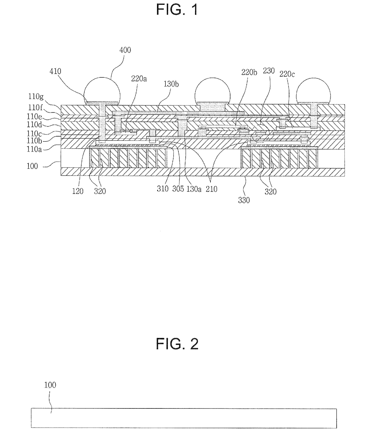
[0032]FIG. 1 illustrates a cross-sectional view of a system-in-package (SiP) according to an embodiment of the present invention.

[0033]The SiP includes a plurality of active devices such as a microprocessor and the like on a substrate 100 obtained by cutting a wafer for each unit system. The active devices may be mounted directly on the top surface of the substrate 100 by a bonding member, or may be buried between multi-layered interlayer dielectrics.

[0034]A passive device may be buried together with the various active devices. The passive device may be formed in t...


PUM


Abstract

There is provided a system-in-package (SiP), which includes a substrate obtained by cutting a wafer for each unit system; one or more first electronic devices mounted on the substrate by a heat radiation plate; a plurality of interlayer dielectrics sequentially formed on the substrate; and one or more second electronic devices buried between or in the interlayer dielectrics on the substrate. A heat sink may be additionally attached to the bottom surface of the substrate. In this case, a thermal conduction path including heat pipes connecting the heat radiation plate on the substrate and the heat sink is formed. In the SiP, various types of devices are buried at a wafer level, so that a more integrated semiconductor device is implemented corresponding to demand for a fine pitch. Further, the heat radiation of a device required in high-speed operation and high heat generation is maximized due to the multi-stepped heat radiation structure, and thus the operation of the device is more stabilized.

Description

BACKGROUND OF THE INVENTION[0001]1. Technical Field[0002]The present invention relates to a system-in-package (SIP) and a fabrication method thereof, and more particularly, to a stack-type package wherein a plurality of electronic devices are buried or stacked on a substrate such as a wafer.[0003]2. Discussion of Related Art[0004]Integration technology for semiconductor devices on a substrate has been continuously developed in order to reduce the size of a system and increase the integration density of semiconductor devices. A system-on-chip (SoC) has been introduced, in which a large number of circuit components are integrated on one chip. However, the SoC, which is configured by stacking various circuits on one single chip, has a technical limit in enhancing circuit integration. Recently, various stack-type structures, such as system-in-package (SiP), system-on-package (SoP), package-on-package (PoP), multi chip package (MCP) and the like, have been suggested as alternatives to ov...

Claims


Application Information

Patent Timeline
Patent Type & Authority Patents(United States)
IPC IPC(8): H01L23/12
CPCH01L21/6835H01L23/3677H01L23/5389H01L24/24H01L24/82H01L24/83H01L2224/83H01L2224/92244H01L2224/73267H01L23/427H01L2221/68345H01L2221/68377H01L2224/24226H01L2224/73253H01L2924/01013H01L2924/01082H01L2924/1433H01L2924/15311H01L2924/19041H01L2924/19042H01L2924/19107H01L2924/30105H01L2924/01006H01L2924/01033H01L2924/014H01L2224/24137H01L2224/32225H01L2924/00H01L2224/04105H01L2224/12105H01L2224/16225H01L2924/19011H01L2924/19104H01L23/12
Inventor PARK, YUN MOOK
Owner NEPES CO LTD
Why Eureka
Try Eureka