Multi-gate semiconductor device and method for forming the same

a semiconductor device and multi-gate technology, applied in the direction of semiconductor devices, basic electric elements, electrical apparatus, etc., can solve the problems of device degradation and/or instability, complex integrated circuits, and incompatibility with current submicron processing techniques, so as to reduce the electrical field, improve hci immunity, and avoid severe hci damage

Active Publication Date: 2011-03-22
NXP USA INC
View PDF4 Cites 6 Cited by
  • Summary
  • Abstract
  • Description
  • Claims
  • Application Information

AI Technical Summary

Benefits of technology

[0033]Still referring to FIG. 10, in an exemplary embodiment, during operation, the source region 58 is grounded and an operational voltage (e.g., approximately 5V) is applied to the drain region 60. The first gate 36 serves as a channel region for the device, and the second gate 38 serves as an extended drain, thus reducing the maximum electric field experienced by the gates 36 and 38. That is, the load of the operational voltage is spread between the first gate 36 and the second gate 38, and as a result, any adverse effects from hot carrier injection (HCI) are greatly reduced.
[0038]As such, the values of the two resistors RT1 and RT2 eventually reverse from RT1>RT2 to RT1<RT2. When this occurs, there is more voltage dropped in the second transistor T2 than in the first transistor T1. Therefore, the second transistor T2, or more specifically the second gate 38, serves as a protective device that limits the actual voltage drop on the first gate 36 (or the first transistor T1) when the supplied drain voltage is higher. The sharing of the drain voltage bias between the first and second transistors T1 and T2 can significantly reduce the electrical field in the gates of 36 and 38, so that the severe HCI damage can be avoided.
[0039]Thus, one advantage of the semiconductor device described above is that the HCI immunity is improved, as the likelihood of any damage and / or performance degradation from HCI current is minimized. Another advantage is that because the structure of the device is self-aligned, the matching performance of the device is improved. A further advantage is that the saturation current of the transistor is increased, as the saturation current is mainly determined by the length of the first gate which can be very small (e.g., 0.2 micron) without the device being damaged by HCI. Therefore, the overall size of the device is effectively decreased. The on-state resistance of the transistor is also reduced because the first gate length can be reduced and the value of the second resistor RT2 is very small when VD is small (i.e., Vg−Vt1<<Vg−Vt2−V12 because Vt1>>Vt2), as the linear drain current is improved compared to a conventional device. A yet further advantage is that the transistor may be constructed using standard complementary metal oxide semiconductor (CMOS) processing steps, thus avoiding increases in manufacturing costs.

Problems solved by technology

In recent years, integrated circuits have become more complicated both in terms of packing density and the variety of device components that are included in a single circuit.
The high kinetic energies cause impact ionization on the semiconductor lattice to generate pairs of electrons and holes moving in random directions with high kinetic energies, which are called “hot carriers.” Some of the hot carriers are injected and trapped in a dielectric within the device (e.g., the gate oxide or silicide block), where they form an undesirable space charge, which can cause device degradation and / or instability.
However, such structures are not compatible with current submicron processing techniques.
However, even with low electric fields, the silicide block experiences significant HCI damage, and the charge trapped within the silicide block causes significant transconductance degradation, as well as the linear current degradation.
The problems associated with HCI are exacerbated as devices continue to get smaller while maintaining relatively high operational voltages (e.g., approximately 5 V).
Because of the problems caused by HCI, conventional device designs, such as those incorporating the extended drains using silicide blocks, may not perform adequately while incorporating the latest submicron (e.g., 0.13 micron) technology platforms.

Method used


Image

  • Multi-gate semiconductor device and method for forming the same
  • Multi-gate semiconductor device and method for forming the same
  • Multi-gate semiconductor device and method for forming the same

Examples


Embodiment Construction

[0019]The following detailed description is merely exemplary in nature and is not intended to limit the invention or application and uses of the invention. Furthermore, there is no intention to be bound by any expressed or implied theory presented in the preceding technical field, background, brief summary, or the following detailed description. It should also be noted that FIGS. 1-12 are merely illustrative and may not be drawn to scale.

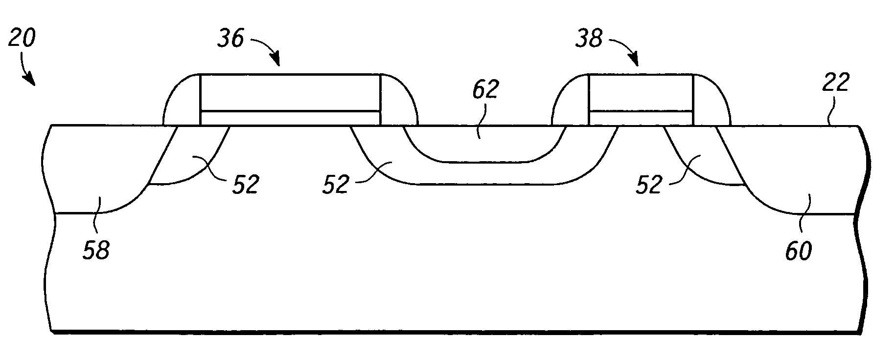
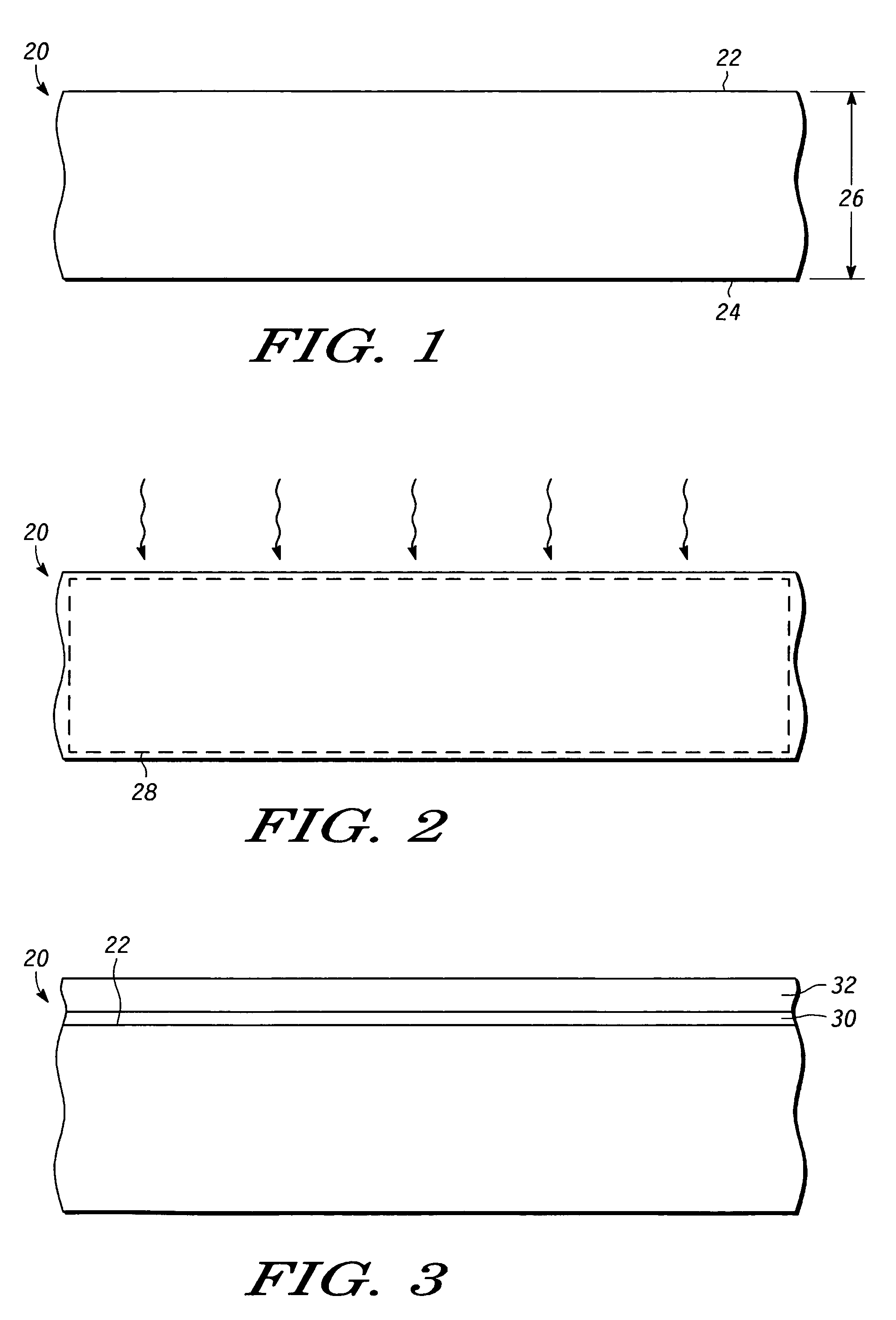
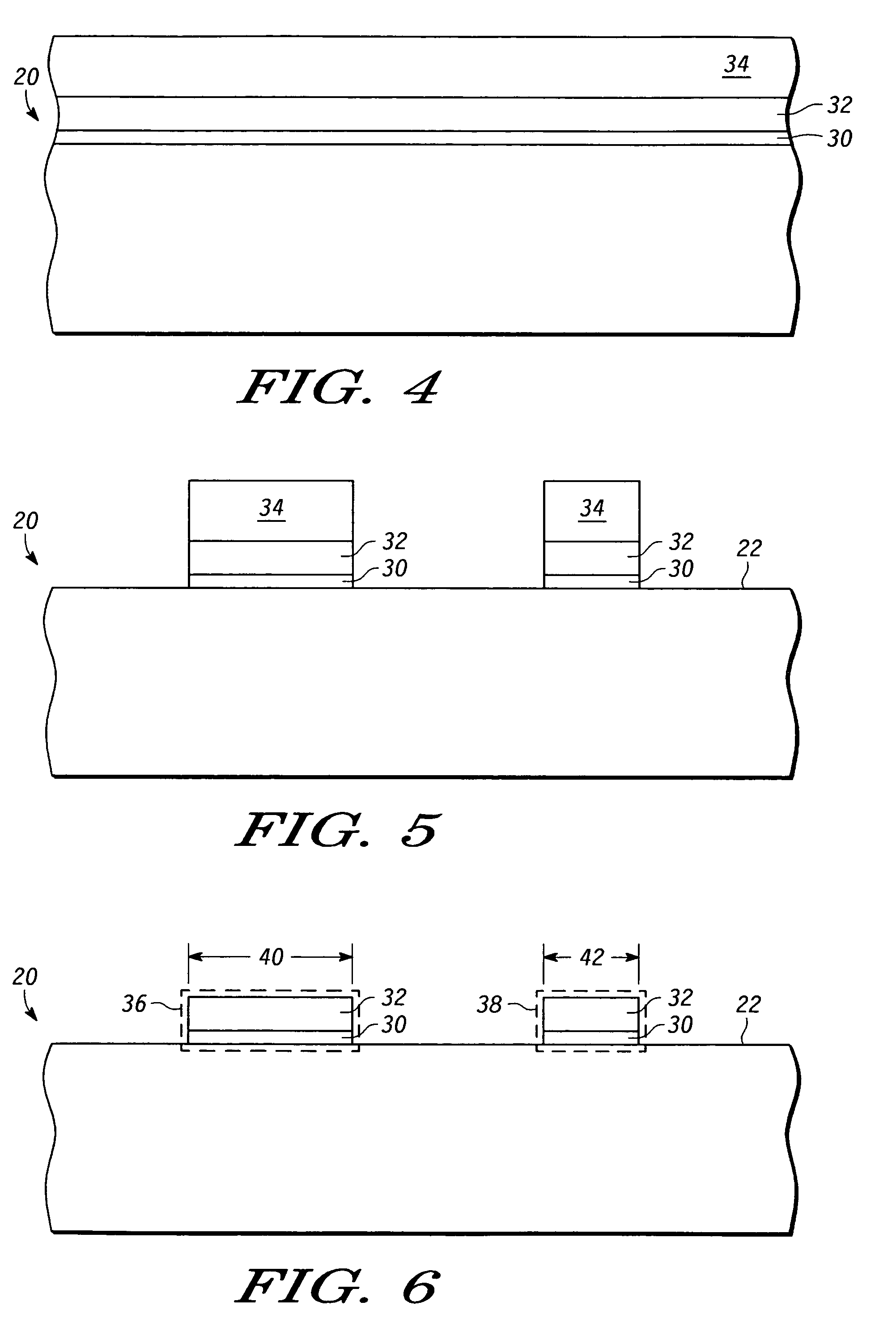
[0020]Referring to FIG. 1, there is illustrated a semiconductor substrate 20. The semiconductor substrate 20 is made of a semiconductor material, such as gallium arsenide (GaAs), gallium nitride (GaN), or silicon (Si). The substrate 20 has an upper surface 22, a lower surface 24, and a thickness 26 of, for example, between approximately 300 and 1000 microns. The semiconductor material of the substrate 20 may be of a first conductivity type, or doped with a first dopant type, and may include an upper layer of epitaxial silicon, as is commonly underst...


PUM


Abstract

A semiconductor device includes a substrate (20), a source region (58) formed over the substrate, a drain region (62) formed over the substrate, a first gate electrode (36) over the substrate adjacent to the source region and between the source and drain regions, and a second gate electrode (38) over the substrate adjacent to the drain region and between the source and drain regions.

Description

FIELD OF THE INVENTION[0001]The present invention generally relates to a semiconductor device and a method for forming a semiconductor device, and more particularly relates to a multi-gate semiconductor device.BACKGROUND OF THE INVENTION[0002]Integrated circuits are formed on semiconductor substrates, or wafers. The wafers are then sawed into microelectronic dies (or “dice”), or semiconductor chips, with each die carrying a respective integrated circuit. Each semiconductor chip is mounted to a package, or carrier substrate, which is often mounted to a motherboard and installed in various electronic systems.[0003]In recent years, integrated circuits have become more complicated both in terms of packing density and the variety of device components that are included in a single circuit. As the productivity and performance demands increase, the size of integrated circuits, as well as the semiconductor chips on which they are formed, continues to be reduced. As the individual devices (e....

Claims


Application Information

Patent Timeline
Patent Type & Authority Patents(United States)
IPC IPC(8): H01L21/8234
CPCH01L29/1041H01L29/66484H01L29/7831H01L29/7833
Inventor YANG, HONGNINGLIN, XINZUO, JIANG-KAI
Owner NXP USA INC
Why Eureka
Try Eureka