Semiconductor package having a crack-propagation preventing unit

a technology of crack propagation and semiconductor package, which is applied in the direction of semiconductor/solid-state device details, semiconductor devices, electrical devices, etc., can solve the problems of mechanical impact brittleness, operational inability of semiconductor devices, and significantly decrease the structural stability of semiconductor chips or semiconductor packages, so as to improve the structural and mechanical intensity and durability of semiconductor packages, notably the wafer level semiconductor packages, the effect of improving the reliability of products

Active Publication Date: 2011-04-05
NEPES CO LTD
View PDF9 Cites 4 Cited by
  • Summary
  • Abstract
  • Description
  • Claims
  • Application Information

AI Technical Summary

Benefits of technology

[0008]This defect is likely to propagate in the semiconductor chip in a subsequent process, to considerably decrease the structural stability of the semiconductor chip or semiconductor package. Moreover, there is a serious problem in that the propagation of the structural defect results in the operational incapability of the semiconductor device.
[0022]In accordance with the present invention, the structural and mechanical intensity and durability of the semiconductor package, specifically, the wafer level semiconductor package, are improved, and the reliability of the product is greatly improved. Furthermore, the thin semiconductor package is prevented from warping, so that the package is easily handled during a subsequent process, such as package mounting, to increase the yield and generally reduce the manufacturing cost. Furthermore, the impact-resistance of brittle materials is improved so that various materials can be used in the packaging process.

Problems solved by technology

When a semiconductor chip or a semiconductor package is formed in a very small size and to a very thin thickness as a semiconductor device has been developed to be light, thin, short and small, it becomes brittle by a mechanical impact.
This defect is likely to propagate in the semiconductor chip in a subsequent process, to considerably decrease the structural stability of the semiconductor chip or semiconductor package.
Moreover, there is a serious problem in that the propagation of the structural defect results in the operational incapability of the semiconductor device.
Then, when a drop test or a physical impact test of applying a mechanical impact is performed, the possibility of the crack or partial chipping becomes high because the edge part of the semiconductor chip is brittle.
The mechanical or structural defect of the semiconductor chip or semiconductor package drops the reliability of the wafer level package process and becomes an obstacle in providing a light, thin, short and small semiconductor device.

Method used


Image

  • Semiconductor package having a crack-propagation preventing unit
  • Semiconductor package having a crack-propagation preventing unit
  • Semiconductor package having a crack-propagation preventing unit

Examples


Embodiment Construction

[0031]The present invention will now be described more fully hereinafter with reference to the accompanying drawings, in which preferred embodiments of the invention are shown.

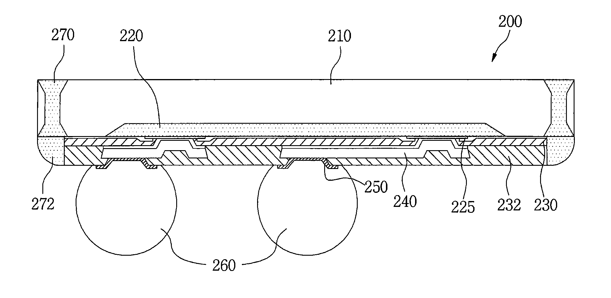
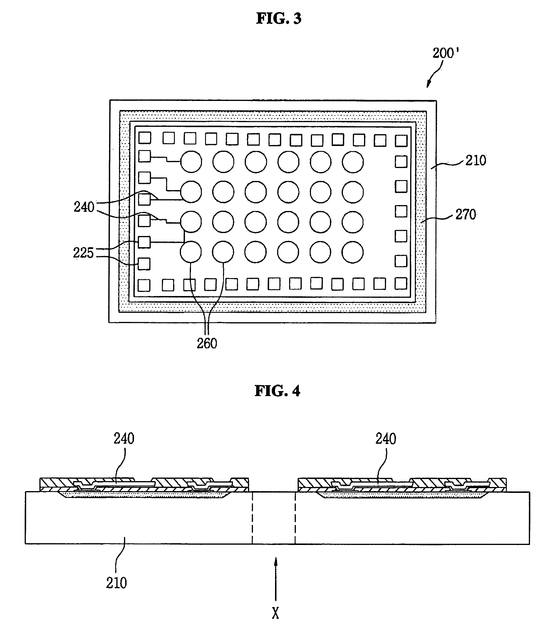
[0032]In a semiconductor package, specifically, a wafer level semiconductor package, according to the present invention, a crack-propagation preventing unit for preventing a physical defect, such as a crack, from propagating toward the inside of a semiconductor chip is provided by forming a trench or moat to surround an outer edge of a semiconductor chip nearby a scribe lane as a sawing part to saw an individual semiconductor chip unit and by filling the inside of the trench or moat with resin, such as epoxy mold, so that the impact-resistance of the semiconductor package is improved.

[0033]Accordingly, when a sawing or dicing process is performed to separate an individual semiconductor chip during a wafer level semiconductor packaging process, although a fine crack or partial chipping occurs, this defect is fu...


PUM


Abstract

There are provided a semiconductor package comprising: a semiconductor substrate including an integrated circuit unit, and a crack-propagation preventing unit at least partially formed around a peripheral of the integrated circuit unit of the semiconductor substrate and filled with a heterogeneous material different from a material of the semiconductor substrate, and a method of fabricating the semiconductor package, comprising: at least partially forming a trench around the peripheral of the integrated circuit unit of the semiconductor substrate, and filling the trench with a heterogeneous material different from that of the semiconductor substrate. In accordance with the present invention, the structural and mechanical strength and durability of the semiconductor package, specifically, the wafer level semiconductor package, are improved and the reliability of the product is significantly improved. Furthermore, a fail rate including crack / chipping during a subsequent mounting process lowers, to improve the yield and reduce the whole manufacturing cost.

Description

CROSS-REFERENCE TO RELATED APPLICATIONS[0001]This U.S. non-provisional patent application claims priority under 35 U.S.C. §119 of Korean Patent Application No. 2007-101343, filed Oct. 9, 2007, the contents of which are incorporated herein by reference in their entirety.FIELD OF TIE INVENTION[0002]The present invention relates to a semiconductor package and a method of fabricating the same, and more particularly, to a new semiconductor package which fundamentally prevents a physical defect such as a crack or partial chipping from propagating within the package.BACKGROUND OF THE INVENTION[0003]A semiconductor device is capable of performing diverse operations with a number of electric devices integrated in a single substrate. For this purpose, various high-technical fabrication methods have been used, and each device in the semiconductor device being fabricated has been developed to be miniaturized as a component in smaller dimensions.SUMMARY[0004]Semiconductor systems of high-integra...

Claims


Application Information

Patent Timeline
Patent Type & Authority Patents(United States)
IPC IPC(8): H01L23/544
CPCH01L23/3185H01L23/562H01L24/03H01L24/05H01L24/13H01L2224/0401H01L2224/16H01L2924/01322H01L2924/14H01L2924/01019H01L2224/0613H01L23/12
Inventor PARK, YUN MOOK
Owner NEPES CO LTD
Why Eureka
Try Eureka