Design methodology for MuGFET ESD protection devices

a technology of protection device and design methodology, which is applied in the direction of detecting faulty computer hardware, instruments, electric digital data processing, etc., can solve the problems of high initial leakage, high complexity, and device with too high initial leakage, so as to achieve better optimization

Inactive Publication Date: 2011-04-12
INTERUNIVERSITAIR MICRO ELECTRONICS CENT (IMEC VZW)
View PDF0 Cites 183 Cited by
  • Summary
  • Abstract
  • Description
  • Claims
  • Application Information

AI Technical Summary

Benefits of technology

[0015]Using the methodology of the invention, better results can be obtained as one might intuitively think. For example, when optimizing towards area, one might think that the best device in MOS diode mode is a wide fin transistor with a minimum gate length which just fulfills the leakage requirements. However, when applying the methodology, the optimal solution turns out to be different, with an area of for example a 20% reduction compared to the intuitive solution. An example to prove the effect of the invention will be presented below.
[0016]In preferred embodiments of the method of the invention, the optimum values are determined by interpolation while taking into account the predetermined ESD constraints and possible other desired specifications of the device.
[0017]In embodiments of the method of the invention, the second set of parameters which can be determined independently from the manufacturing process can comprise one or more of the following layout parameters: a contact area (Lcont) and a folding factor of the ESD protection device.
[0018]In embodiments of the method of the invention, the following layout parameters can belong to either the first set (fixed by the manufacturing process) or the second set (independent from the manufacturing process), depending on the manufacturing process which is used: a distance between landing pad and gate (LSD), an overlap gate on fins (Wext) and a fin-to-fin spacing (S).
[0019]In embodiments of the method of the invention, the following process parameters can belong to either the first set (fixed by the manufacturing process) or the second set (independent from the manufacturing process), depending on the manufacturing process which is used: strain, well implants, selective epitaxial growth (SEG), silicide blocking.
[0020]In embodiments of the method of the invention, the following parameters can belong to the subset of at least one parameter to be optimized: overall area of said device, maximum voltage, maximum voltage during voltage overshoot, leakage current, capacity.

Problems solved by technology

Major challenges lie ahead for the ESD design engineer.
A design methodology is needed because the more complex geometry of FinFET devices compared to planar introduces a higher degree of complexity that make optimization absolutely not obvious as compared to planar devices.
For wide fin (planar) devices (FIG. 2 dotted lines) for small gate lengths, a VT roll-off is seen because of loss of SCE control.
Devices with too high initial leakage would consequently have a low ESD robustness, and hence are not considered.
It2 and Ron may be impacted by constraints in the metal wiring and / or accumulative heating of folded structures.
It is clear that any LG or Wfin deviation from the optimum leads to a drastic increase in the required area.
No solutions exist for small LG because of the leakage current limitation and for large LG because of too high voltage drop.
This solution is limited by the leakage current limit and results in an increased area consumption of 40%, namely 417 μm2.
On the contrary, for wide fin devices VT decreases with short gate lengths, thus these devices have poor control of SCE and hence cannot be used.
Ron-extraction in diode mode is more difficult than in bipolar mode due to the non-linear current behavior (FIG. 2).
However, the overall performance of the MOS diode is not superior to the bipolar mode, which is generally the case.
This has an important consequence, namely that in some cases, the MOS diode mode would become the limiting factor when compared to the bipolar mode.
However, when technology keeps evolving, the different dependencies might change, making the design methodology necessary.
However, concluding from these results that the best ESD device would be a device with wide fins is not correct.
For narrow fin devices, VT is determined by the workfunction of the metal gate since the full depletion makes tuning of VT with implantation very difficult.
As a consequence, such a wide fin device can meet leakage requirements with a smaller Lg which directly results in reduced Vh and Ron.
Since these devices fail non-uniformly due to isothermal current instability at high current levels, constant current density simulations are used instead of constant power.
Obviously, forcing the same amount of current through a thinner silicon film leads to increased heating.
The thicker TBOX clearly prevents heat transfer to the substrate and hence causes increased heating of the silicon fins.

Method used


Image

  • Design methodology for MuGFET ESD protection devices
  • Design methodology for MuGFET ESD protection devices
  • Design methodology for MuGFET ESD protection devices

Examples


Embodiment Construction

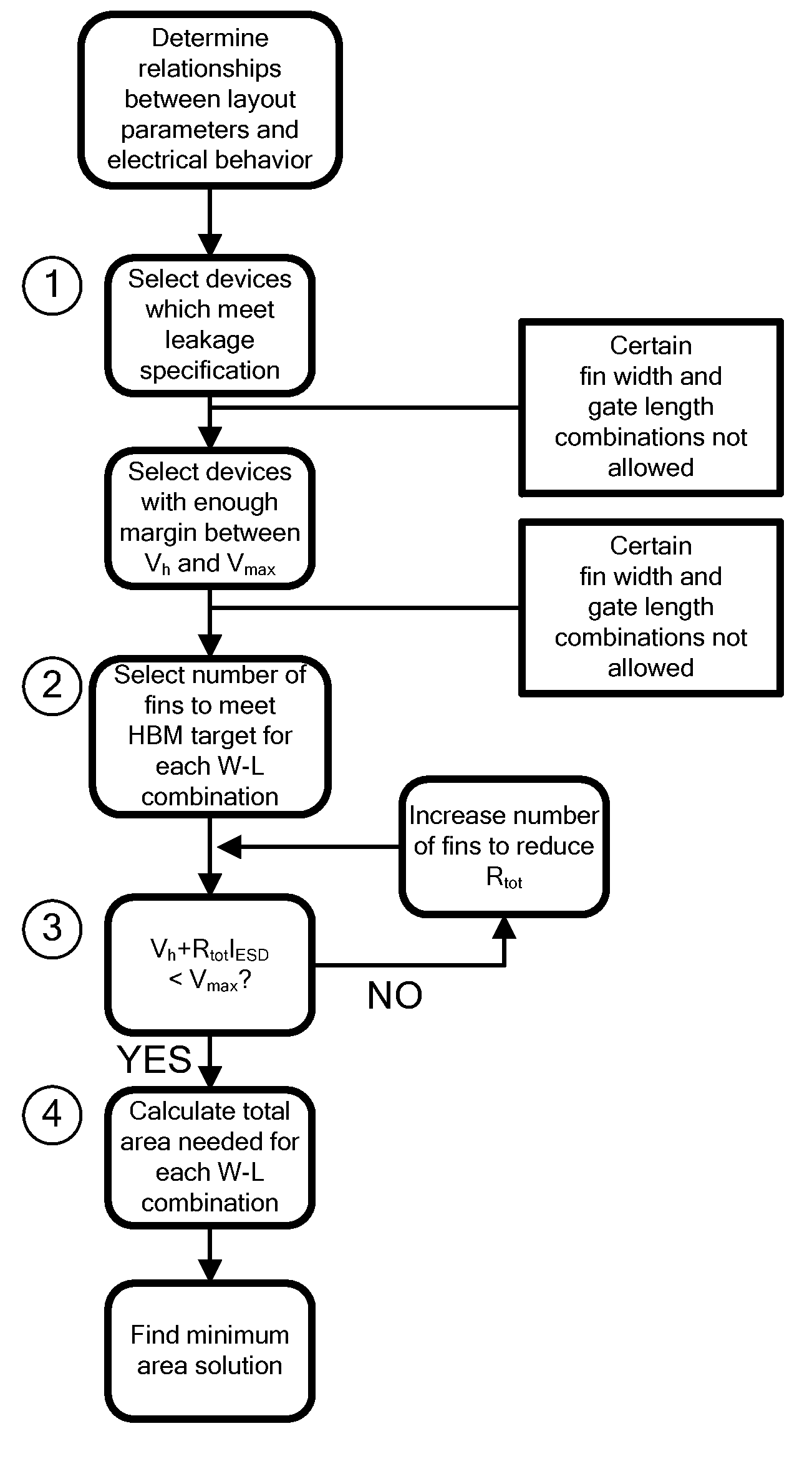
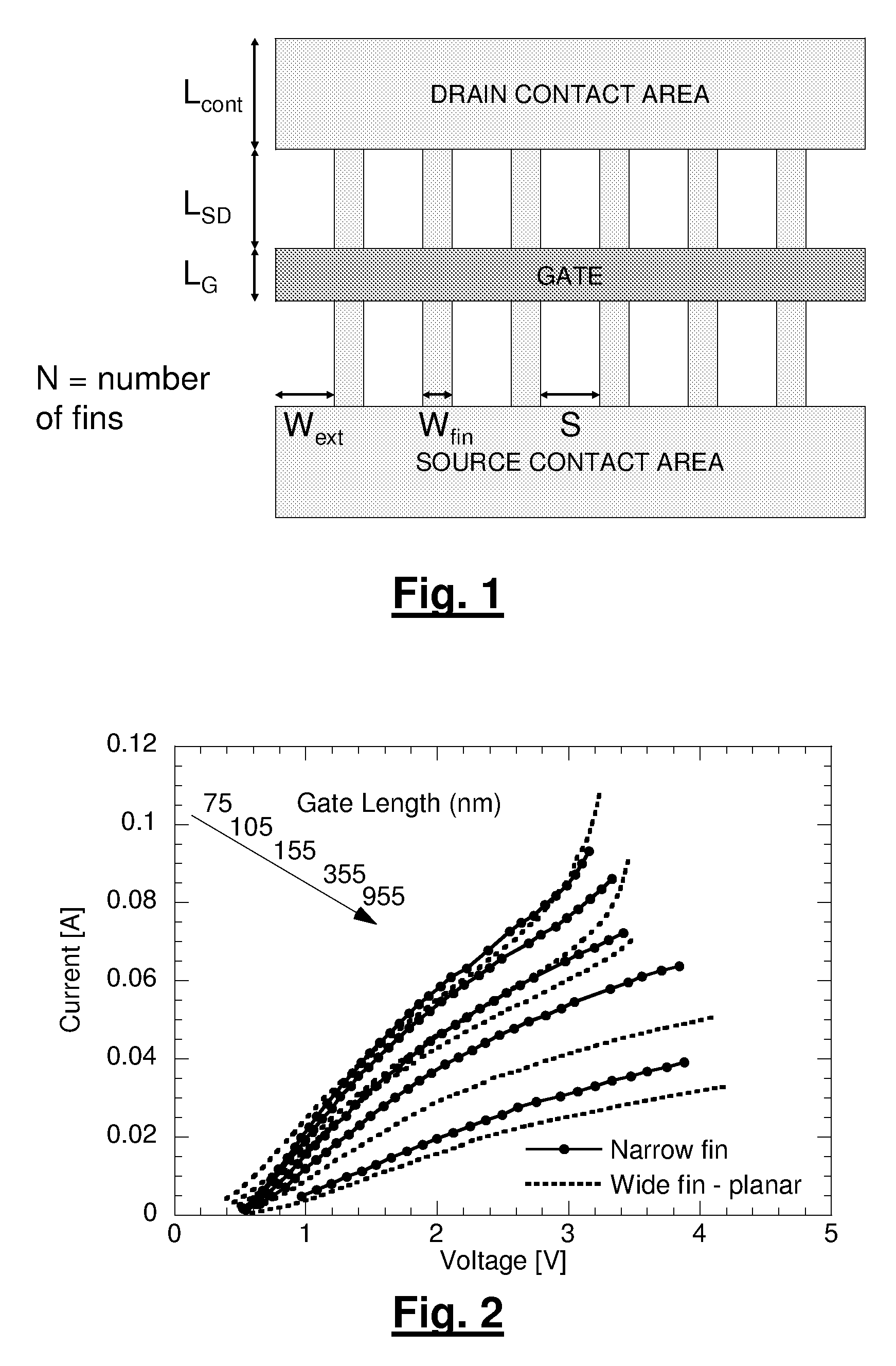
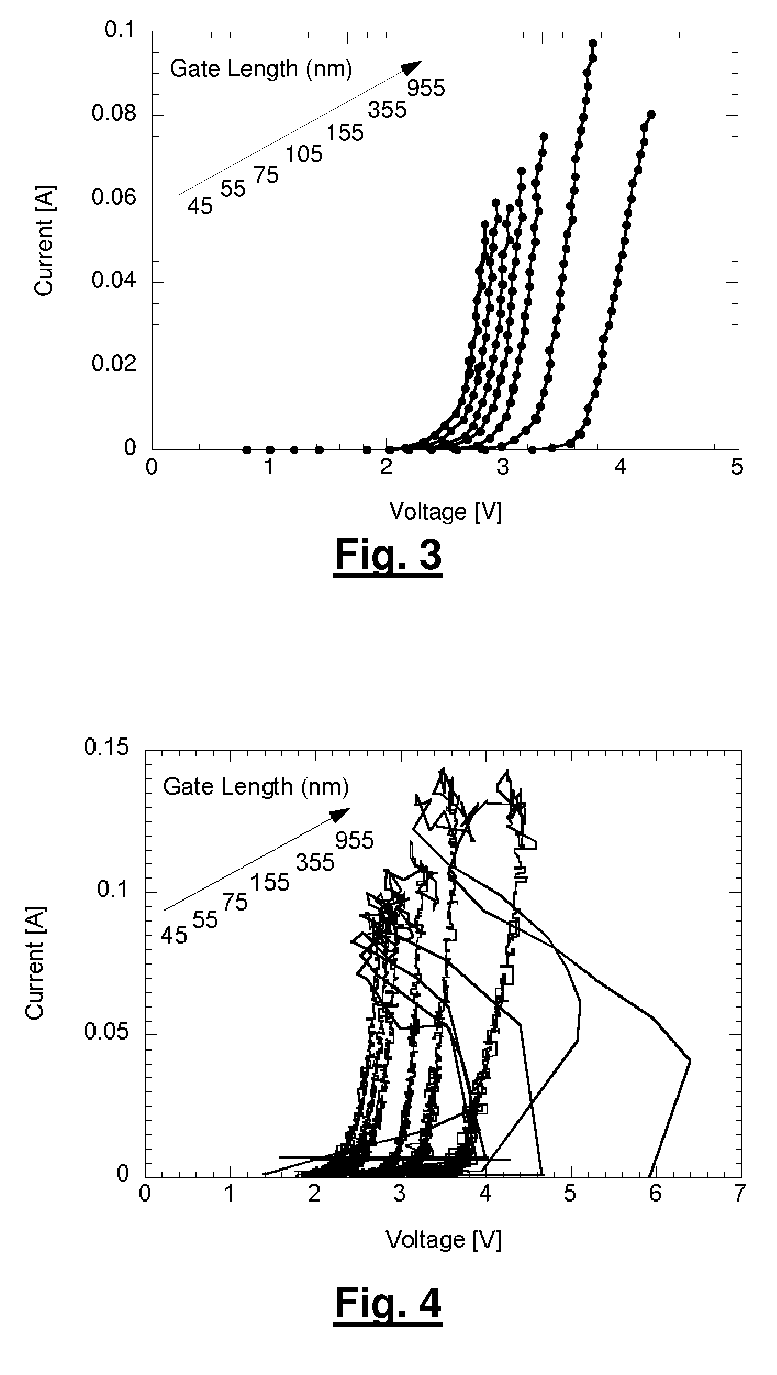
[0060]The present invention will be described with respect to particular embodiments and with reference to certain drawings but the invention is not limited thereto but only by the claims. The drawings described are only schematic and are non-limiting. In the drawings, the size of some of the elements may be exaggerated and not drawn on scale for illustrative purposes. The dimensions and the relative dimensions do not necessarily correspond to actual reductions to practice of the invention.

[0061]Furthermore, the terms first, second, third and the like in the description and in the claims, are used for distinguishing between similar elements and not necessarily for describing a sequential or chronological order. The terms are interchangeable under appropriate circumstances and the embodiments of the invention can operate in other sequences than described or illustrated herein.

[0062]Moreover, the terms top, bottom, over, under and the like in the description and the claims are used fo...


PUM


Abstract

A method for manufacturing a MuGFET ESD protection device having a given layout by means of a given manufacturing process, the method comprising selecting multiple interdependent layout and process parameters of which a first set are fixed by said manufacturing process and a second set are variable, selecting multiple combinations of possible layout and process parameter values which meet predetermined ESD constraints; determining an optimum value for at least one other parameter in view of a predetermined design target apart from the predetermined ESD constraints; determining values for fin width (Wfin), gate length (LG) and number of fins (N) on the basis of the optimum value; and manufacturing said MuGFET ESD protection device using the given manufacturing and process values.

Description

CROSS-REFERENCE TO RELATED APPLICATIONS[0001]The present application claims priority to European Patent Application EP 08156029.4 filed in the EPO Patent Office on May 9, 2008, the entire contents of which is incorporated herein by reference.BACKGROUND[0002]1. Field of the Invention[0003]The present invention relates to designing and manufacturing MuGFET ESD Protection Devices.[0004]2. Description of the Related Art[0005]The FinFET transistor is the most widely studied multi-gate architecture for technology-scaling below 45 nm due to its excellent control of Short Channel Effects (SCE) and its compatibility with standard CMOS processing. In Trémouilles et al, “Understanding the Optimization of Sub-45 nm MuGFET Devices for ESD Applications”, ESD 2007, pp 408-415, a variety of ESD device parameters (failure current It2, holding voltage Vh, on-resistance Ron, leakage current and area consumption) of a Grounded-Gate-NMOS FinFET device were investigated as a function of different layout ...

Claims


Application Information

Patent Timeline
Patent Type & Authority Patents(United States)
IPC IPC(8): H01L21/66H01L21/00H01L21/84H01L21/336H01L21/332
CPCH01L27/0248H01L29/66795
Inventor THIJS, STEVENLINTEN, DIMITRITREMOUILLES, DAVID ERIC
Owner INTERUNIVERSITAIR MICRO ELECTRONICS CENT (IMEC VZW)
Why Eureka
Try Eureka