Stable gold bump solder connections

a solder connection and gold bump technology, applied in the field of metalurgical systems, can solve the problems of aluminum/gold intermetallics loss, aluminum pad loss, aluminum pad loss, etc., and achieve the effect of stabilizing the remaining gold bump

Active Publication Date: 2011-05-10
TEXAS INSTR INC
View PDF6 Cites 33 Cited by
  • Summary
  • Abstract
  • Description
  • Claims
  • Application Information

AI Technical Summary

Benefits of technology

[0008]In the analysis of the solder contacts, applicants further discovered that, after implementing a nickel layer to cover the copper contact and to practically eliminate the copper diffusion into the solder, the gold / tin intermetallics can be stabilized as distinct regions. They form “coating” layers around the gold bump, reducing additional gold dissolution during subsequent reflow processes. They thus preserve the remaining gold bump as soft, stress-mitigating material to pass mechanical tests. In addition, the gold preserved after the assembly processes will be large enough to withstand gold solid-state dissolution into solder during prolonged high temperature storage or field application. With less gold dissolved into the solder, the volume fraction of gold / tin intermetallics in solder is smaller and thus the joint less brittle.

Problems solved by technology

Because of the brittleness of these compounds and the direct contact of the intermetallics with the aluminum pad on the chip side, the joints frequently fail reliability tests such as the mechanical drop test by cracking at the bump / chip interface.
For chips which have the gold bumps positioned on an aluminum layer, an additional problem appears after the consumption of the gold bump: In consecutive reflow operations (for many devices, three more reflows are needed), the aluminum / gold intermetallics may also be lost so that the aluminum pad loses its solderablity altogether.

Method used


Image

  • Stable gold bump solder connections
  • Stable gold bump solder connections
  • Stable gold bump solder connections

Examples


Embodiment Construction

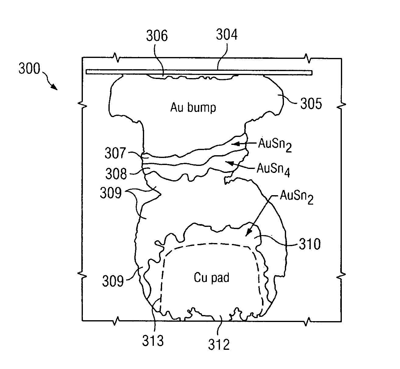
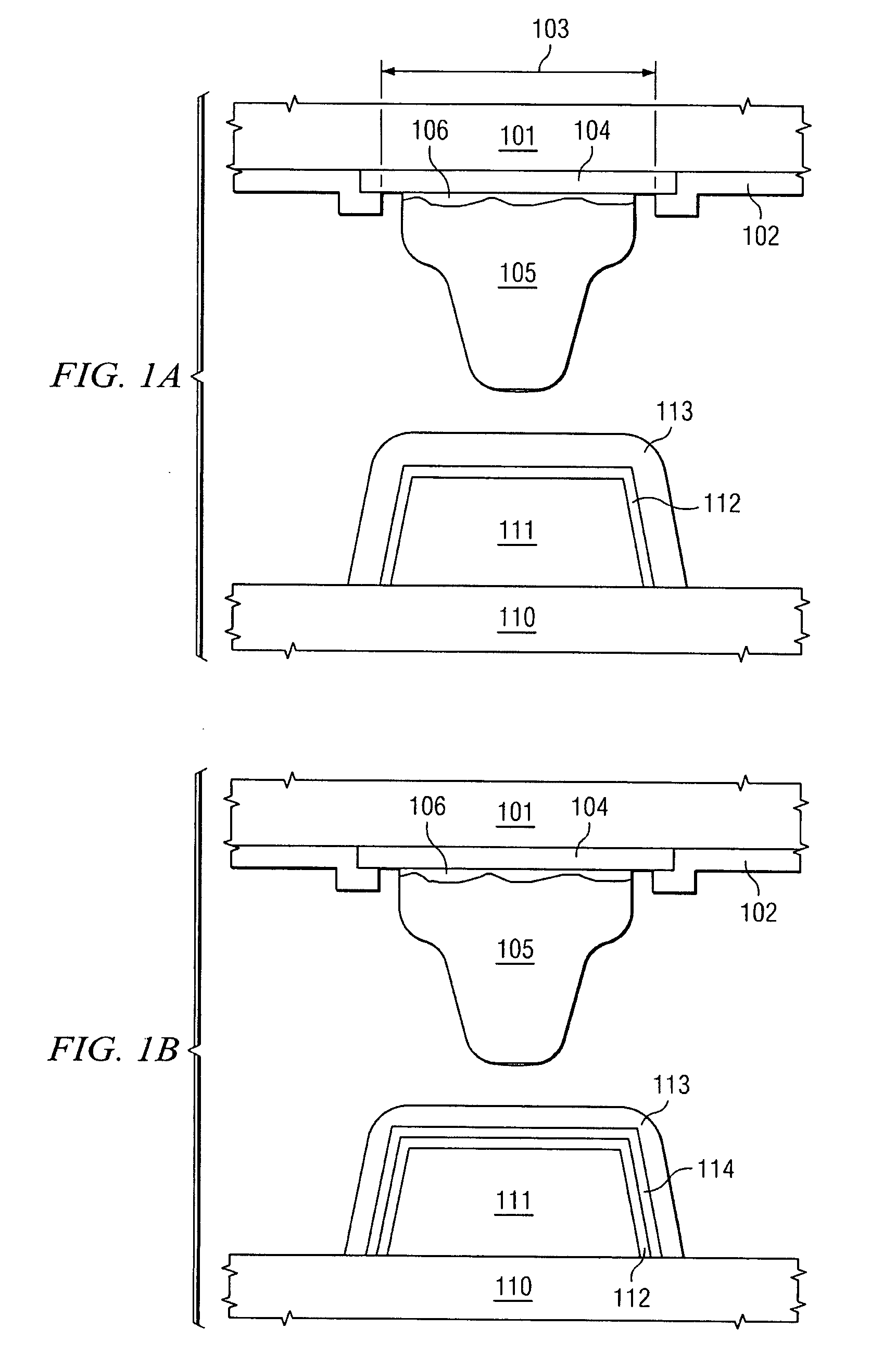
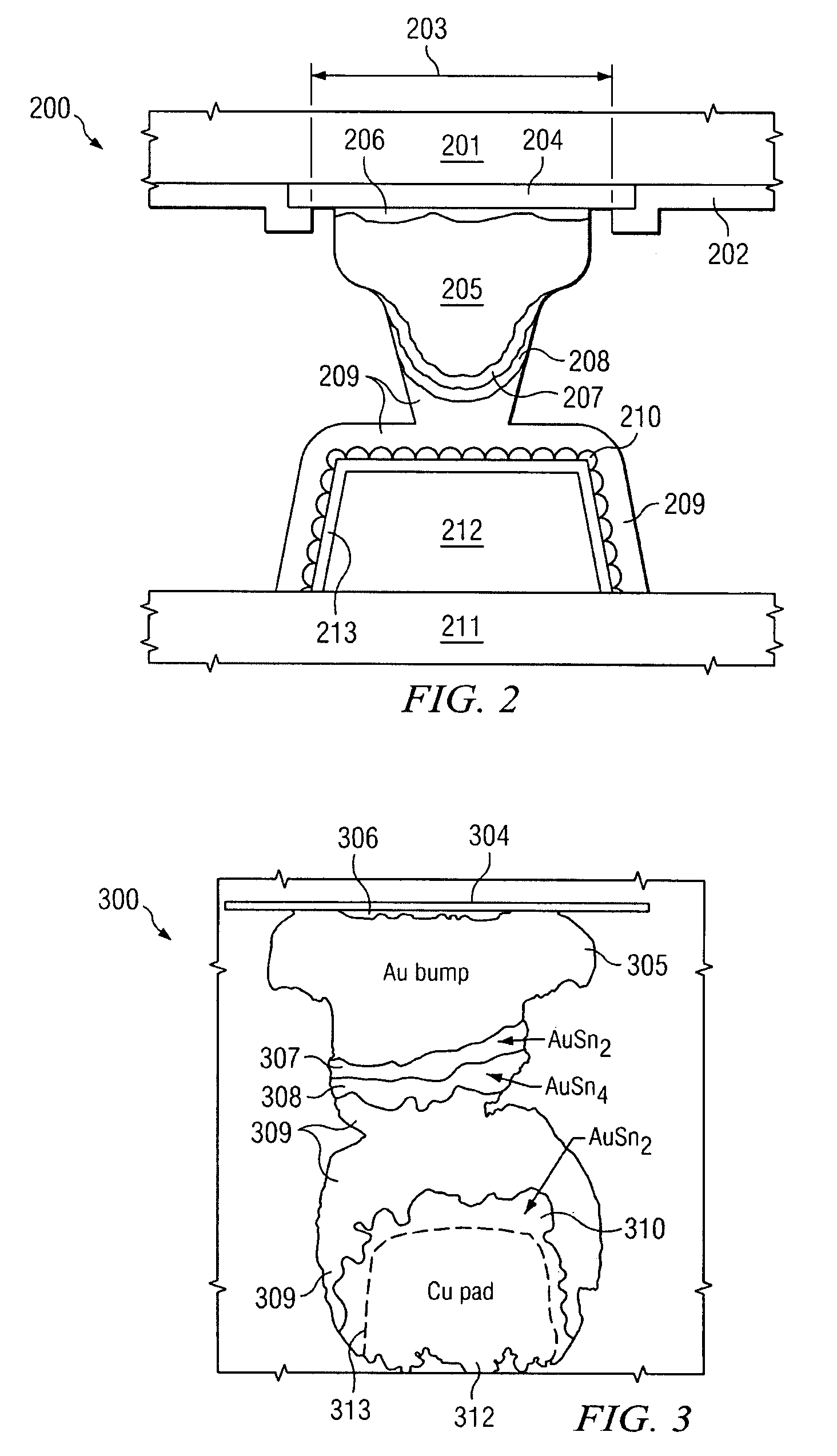
[0023]An embodiment of the invention is a metallic interconnect structure for connecting a gold bump and a copper pad. FIGS. 1A and 1B show the gold bump and the copper pad before forming the interconnect structure. In FIG. 1A, a portion of a semiconductor chip 101 has an insulating overcoat 102 (for example, silicon nitride or oxynitride) with a window 103 in the overcoat. The window exposes a portion of chip metallization 104, which is preferably aluminum or aluminum alloy with a surface bondable to gold. Alternatively, metallization 104 may be made of copper; again, the surface of pad 104 needs to be bondable to gold. For example, the surface of pad 104 may have a thin layer of gold or palladium. The exposed metal in window 103 serves as a pad for electrical and mechanical contact to chip 101.

[0024]Attached to contact pad 104 is a stud, or bump, 105, preferably made of gold. Due to the fabrication method, bump 105 may have the shape of a deformed sphere. At the interface between ...


PUM

PropertyMeasurementUnit
thicknessaaaaaaaaaa
thickaaaaaaaaaa
thickaaaaaaaaaa

Abstract

A metallic interconnect structure (200) for connecting a gold bump (205) and a copper pad (212), as used for example in semiconductor flip-chip assembly. A first region (207) of binary AuSn2 intermetallic is adjacent to the gold bump. A region (208) of binary AuSn4 intermetallic is adjacent to the first AuSn2 region. Then, a region (209) of binary gold-tin solid solution is adjacent to the AuSn4 region, and a second region (210) of binary AuSn2 intermetallic is adjacent to the solid solution region. The second AuSn2 region is adjacent to a nickel layer (213) (preferred thickness about 0.08 μm), which covers the copper pad. The nickel layer insures that the gold / tin intermetallics and solutions remain substantially free of copper and thus avoid ternary compounds, providing stabilized gold bump / solder connections.

Description

FIELD OF THE INVENTION[0001]The present invention is related in general to the field of metallurgical systems with application to electronic systems and semiconductor devices, and more specifically to stable gold bump solder connections.DESCRIPTION OF THE RELATED ART[0002]The growing popularity of flip-chip assembly in the fabrication process flow of silicon integrated circuit (IC) devices is driven by several facts. First, the electrical performance of the semiconductor devices can be improved when the parasitic inductances correlated with conventional wire bonding interconnection techniques are reduced. Second, flip-chip assembly provides higher interconnection densities between chip and package than wire bonding. Third, flip-chip assembly consumes less silicon “real estate” than wire bonding, and thus helps to conserve silicon area and reduce device cost. And fourth, the fabrication cost can be reduced, when concurrent gang-bonding techniques are employed rather than consecutive ...

Claims


Application Information

Patent Timeline
Patent Type & Authority Patents(United States)
IPC IPC(8): H01L23/52
CPCB23K1/0016B23K35/007B23K35/262B23K35/286B23K35/3013H01L23/49811H01L24/11H01L24/12H01L24/16H01L24/81H01L25/105H01L2224/1134H01L2224/13144H01L2224/13147H01L2224/13583H01L2224/136H01L2224/13644H01L2224/13655H01L2224/16225H01L2224/73204H01L2224/81193H01L2224/8121H01L2224/81815H01L2225/06558H01L2225/06568H01L2924/01004H01L2924/01012H01L2924/01013H01L2924/0102H01L2924/01029H01L2924/01032H01L2924/01046H01L2924/01047H01L2924/01078H01L2924/01079H01L2924/01082H01L2924/01327H01L2924/14H01L2924/15311H01L2924/15331H01L2924/30107H01L2924/3025H01L2224/0558H01L2224/05644H01L2924/00013H01L2924/01006H01L2924/01033H01L2924/0105H01L2924/014H01L2225/1023H01L2225/1058H01L2224/0401H01L2924/00014H01L2224/13099H01L2924/00H01L2224/05124H01L2224/05147H01L2224/05664H01L24/05H01L2924/013
Inventor ZENG, KEJUNPENG, WEI QUNHOLFORD, REBECCA L.FURTAW, ROBERT JOHNGALLEGOS, BERNARDO
Owner TEXAS INSTR INC
Why Eureka
Try Eureka