Inverse resist coating process

a technology of resist coating and inverse resist, which is applied in the field of lithographic, can solve the problems of limiting the minimum feature size of lithographic processes and the unsatisfactory need for a process that overcomes feature size limitations, and achieves the effects of reducing feature size, sublithographic features, and reducing feature siz

Inactive Publication Date: 2011-05-17
GLOBALFOUNDRIES INC
View PDF18 Cites 9 Cited by
  • Summary
  • Abstract
  • Description
  • Claims
  • Application Information

AI Technical Summary

Benefits of technology

[0006]The invention provides systems and processes that form the inverse (photographic negative) of a patterned first coating. The process employs a patterned first coating, which is usually provided by a resist. After the first coating is patterned, a coating of a second material is provided thereover. The uppermost layer of the second coating is removed, where appropriate, to expose the patterned first coating. The patterned first coating is subsequently removed, leaving the second coating material in the form of a pattern that is the inverse pattern of the first coating pattern. The process may be repeated with a third coating material to reproduce the pattern of the first coating in a different material. Prior to applying the second coating, the patterned first coating may be trimmed by etching, thereby reducing the feature size and producing sublithographic features. Another option to reducing feature sizes is to trim the second coating. In addition to providing sublithographic features, the invention gives a simple, efficient, and high fidelity method of obtaining inverse coating patterns. Furthermore, the invention can be used to form a high resolution pattern using a high resolution coating material and then replace the high resolution coating material with another material having superior properties, such as superior dry etch resistance, while retaining the high resolution pattern.

Problems solved by technology

Lithographic processes are generally limited as to minimum feature size.
These limitations are primarily based on the type of resist used and the wavelength of exposing radiation.
There has been an unsatisfied need for a process that overcomes feature size limitations and permits the patterning or formation of extremely small (sub-micron) sub-lithographic features, especially using currently available resist materials and radiation sources.

Method used


Image

  • Inverse resist coating process
  • Inverse resist coating process
  • Inverse resist coating process

Examples


example i

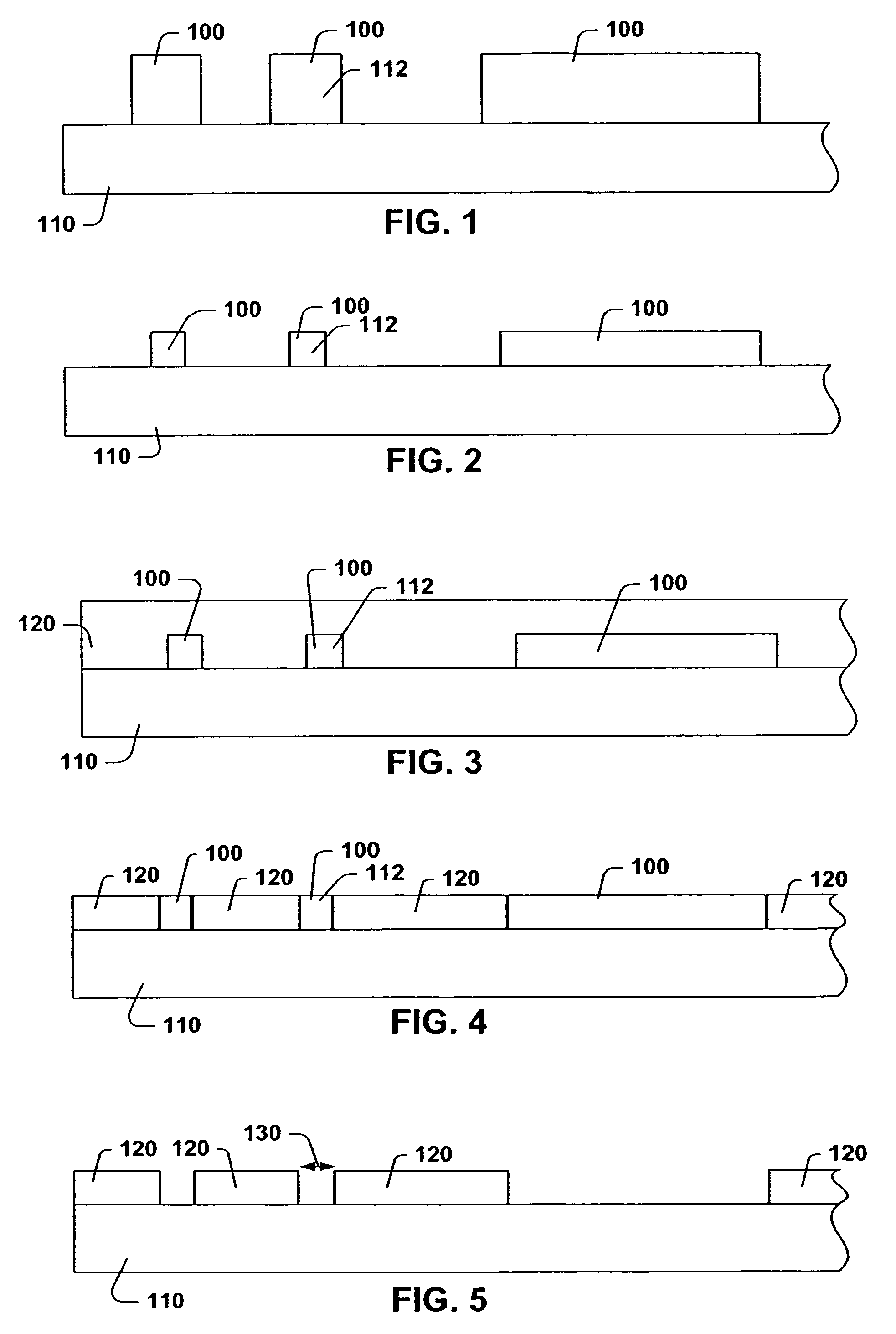
[0054]A process according to one aspect of the invention including an optional trim step is illustrated in FIGS. 1 to 5. FIG. 1 illustrates substrate 110 with patterned first coating 100. In this example, patterned first coating 100 is a positive tone resist that has an aqueous alkali developer. For example, patterned first coating 100 can be a novolac or TOBC. Patterned first coating 100 is formed by coating substrate 110 with a resist solution, prebaking the resist, irradiating the resist through a mask, and developing the resist with an aqueous alkali developer.

[0055]FIG. 2 illustrates patterned first coating 100 after trimming. In this example, trimming is carried out with plasma or reactive ion etching using oxygen and optionally an inert gas. Trimming thins and narrows the features of patterned coating 100 to about half their original size. For example, the width of feature 112, which is a line, is narrowed from a width of about 0.5 μm to a width of about 0.25 μm.

[0056]Prior t...

example ii

[0060]This example uses the procedures of Example I, except for the following: The first coating is positive tone resist having a non-polar organic solvent developer, PMMA or POS for example. The patterned first coating is not irradiated with actinic radiation until after the planarization step. After irradiation, the second coating is removed with a xylene developer.

[0061]In this example, an alternative for the second coating material is a positive tone photoresist, such as a novolac or TOBC. If TOBC is the second coating material, it is irradiated with actinic radiation prior to removal of the patterned first coating.

example iii

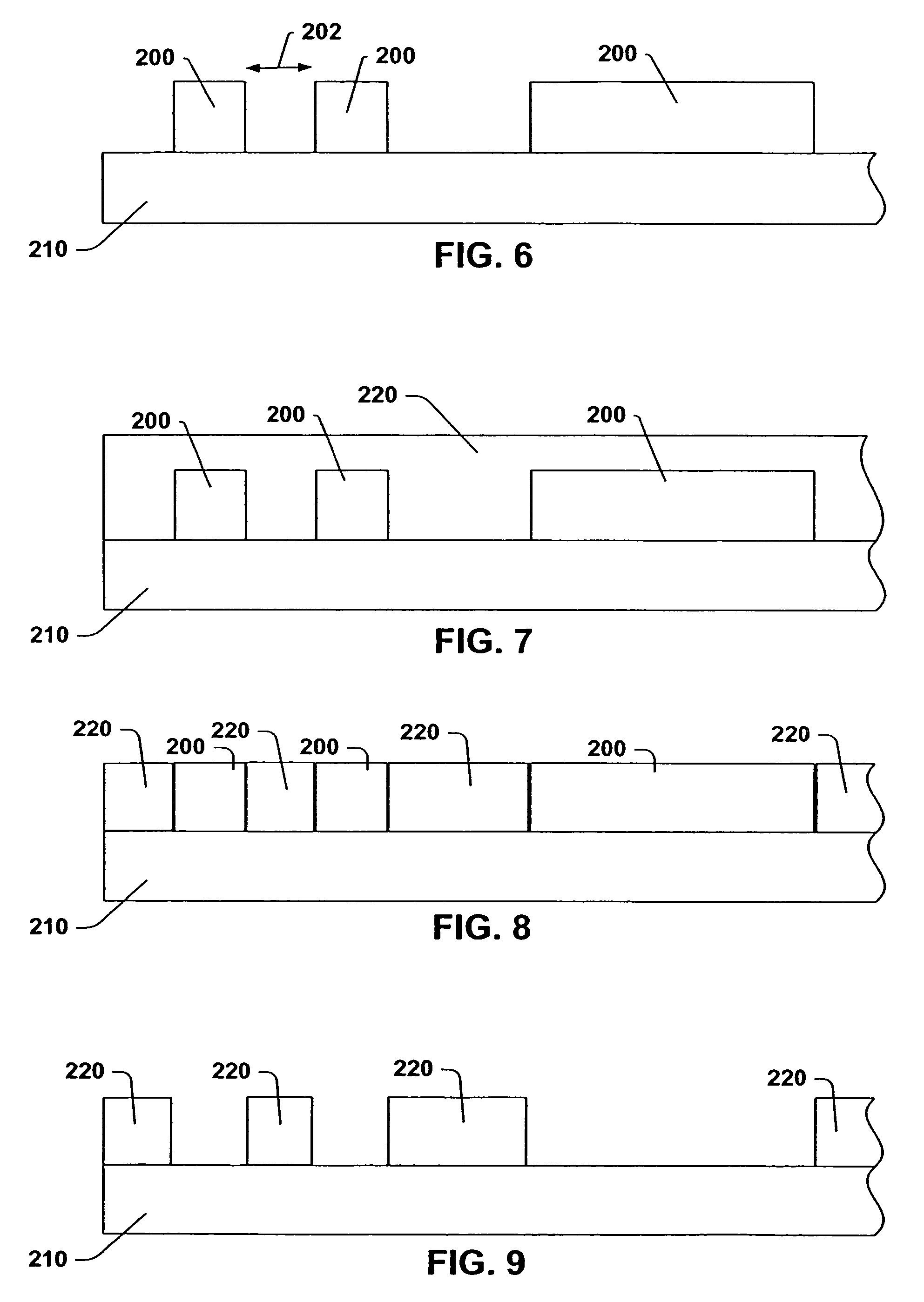
[0062]A process according to another aspect of the invention is illustrated in FIGS. 6 to 9. FIG. 6 shows a patterned first coating 200 formed on substrate 210. Patterned first coating 200 is also a positive tone resist that has an aqueous alkali developer, for example, a novolac or TOBC. Patterned first coating 200 is formed by coating substrate 210 with a resist solution, prebaking the resist, irradiating the resist through a mask, and developing the resist with an aqueous alkali developer.

[0063]Prior to application of the second coating, patterned first coating 200 is irradiated with actinic radiation rendering it soluble in aqueous base. In the case where patterned first coating 200 is TOBC, irradiation renders the coating insoluble in non-polar organic solvent.

[0064]FIG. 7 illustrates second coating material 220 covering the exposed portions of substrate 210 and patterned first coating 200. In this example, second coating 220 is another positive tone resist. Second coating 220 ...


PUM

PropertyMeasurementUnit
temperatureaaaaaaaaaa
feature sizesaaaaaaaaaa

Abstract

The invention provides systems and processes that form the inverse (photographic negative) of a patterned first coating. The patterned first coating is usually provided by a resist. After the first coating is patterned, a coating of a second material is provided thereover. The uppermost layer of the second coating is removed, where appropriate, to expose the patterned first coating. The patterned first coating is subsequently removed, leaving the second coating material in the form of a pattern that is the inverse pattern of the first coating pattern. The process may be repeated with a third coating material to reproduce the pattern of the first coating in a different material. Prior to applying the second coating, the patterned first coating may be trimmed by etching, thereby reducing the feature size and producing sublithographic features. In addition to providing sublithographic features, the invention gives a simple, efficient, and high fidelity method of obtaining inverse coating patterns.

Description

CROSS REFERENCE TO RELATED APPLICATION[0001]This application is a divisional of U.S. application Ser. No. 09 / 973,240, entitled Inverse Resist Coating Process and filed on Oct. 9, 2001 now abandoned, the entirety of which is incorporated herein by reference.TECHNICAL FIELD[0002]The present invention generally relates to semiconductor processing, and in particular to a lithographic process and system for producing patterned coatings having reduced feature sizes.BACKGROUND OF THE INVENTION[0003]In the semiconductor industry, there is a continuing trend toward higher device densities. To achieve these high densities there has been, and continues to be, efforts toward scaling down the device dimensions (e.g., at submicron levels) on semiconductor wafers. In order to accomplish such high device packing density, smaller and smaller features sizes are required. This may include the width and spacing of interconnecting lines, spacing and diameter of contact holes, and the surface geometry su...

Claims


Application Information

Patent Timeline
Patent Type & Authority Patents(United States)
IPC IPC(8): G03F7/20G03F7/40H01L21/027H01L21/033
CPCG03F7/40H01L21/0331H01L21/0274H01L21/0272
Inventor RANGARAJAN, BHARATHTEMPLETON, MICHAEL K.SUBRAMANIAN, RAMKUMAR
Owner GLOBALFOUNDRIES INC
Why Eureka
Try Eureka