Tunable integrated circuit design for nano-scale technologies

a nano-scale technology and integrated circuit technology, applied in the direction of discrete pre-tuned circuits, memory systems, electric pulse generators, etc., can solve the problems of high manufacturing cost, difficult, if not impossible, to create reliable, robust design over all process variations, etc., to facilitate robust integrated circuit design, reduce random mismatches, high-performance and reliable

Inactive Publication Date: 2011-05-17
CARNEGIE MELLON UNIV
View PDF27 Cites 12 Cited by
  • Summary
  • Abstract
  • Description
  • Claims
  • Application Information

AI Technical Summary

Benefits of technology

[0038]The present invention is a post-silicon tuning methodology to reduce random mismatches for analog circuits, which targets the creation of a new tunable integrated circuit (IC) design methodology to accommodate large-scale process variations in nano-scale technologies (e.g., sub-90 nm CMOS). The present invention proposes a new tunable methodology that facilitates robust integrated circuit design in nano-scale technologies based on stochastic technique to address such nano-scale design challenges. The disclosed robust design framework is able to create high-performance and reliable integrated circuits with consideration of large-scale process variations, which is a necessary condition to enable further technology scaling for 65 nm and below.
[0039]The present invention is an adaptive post-silicon tuning approach to reduce random device mismatches. Instead of over-sizing analog devices, a methodology is proposed that would decompose each device into N fingers and adaptively select the best-matched M (M≦N) fingers based on the post-silicon measurement. Such post-silicon tuning was previously applied to several analog design examples (see Background references [14]-[15]). The objective of this invention is to develop a generalized methodology for post-silicon tuning that can be applied to a broad range of application domains. To do so, tunable analog designs are systematically analyzed and optimized, and these designs demonstrate the substantial benefit offered by post-silicon tuning as compared to simple sizing following the Pelgrom model.
[0041]To optimally select M fingers out of N (M≦N) candidates, the number of possible combinations increases exponentially with N, thereby making such a discrete selection problem non-trivial to solve. The proposed DP algorithm partitions the complicated optimization problem into multiple, interacted sub-problems. Instead of directly searching all N fingers, the sub-problem is defined to optimally select j fingers out of i (j≦i) candidates where i is initially set to 1 and it is iteratively increased to N. The sub-problem is solved once and its answer is saved, thereby avoiding the work of re-computing the answer every time when the sub-problem is encountered.
[0042]In addition, the present invention proposes to utilize quantization to efficiently lump many similar selection options together as a single DP state, thereby further reducing the computational complexity. As will be demonstrated by the numerical examples below, even for small-size problems (N=10˜14), the proposed DP algorithm achieves 10˜20× speed-up compared with a brute-force search.

Problems solved by technology

The continued scaling of CMOS technologies has brought about increasing uncertainties in process parameters to the point for which it is difficult to create reliable, robust design over all process variations.
As integrated circuits continue to aggressively scale to smaller feature size (e.g., 65 nm, 45 nm, etc.), it is extremely difficult, if not impossible, to reliably manufacture circuits while achieving high product yield (or equivalently, low manufacturing cost).
As performance margins are increased, however, achieving high-performance IC design quickly becomes infeasible.
The expectation is that this problem will only worsen for post-CMOS technologies.
As previously stated, such schemes ultimately reach a point for which achieving high-performance design becomes infeasible.
As integrated circuit (IC) technologies scale to 65 nm and beyond, process variations become increasingly critical and make it continually more challenging to create a reliable, robust design with high yield (see Background reference [1]).
With scaling of CMOS below 90 nm, the traditional statistical design methodologies attempt to reserve larger performance margins than ever before, thereby making it extremely difficult (or even infeasible) to achieve a high-performance circuit design.
These analog circuits are designed to be robust to inter-die variations, but they are extremely sensitive to device mismatches.
This fundamental limitation prevents analog and RF circuits from further CMOS scaling to achieve smaller area, faster speed and lower power.
The challenging problem is how to more effectively reduce random mismatches such that smaller devices can be used to achieve better performance.

Method used


Image

  • Tunable integrated circuit design for nano-scale technologies
  • Tunable integrated circuit design for nano-scale technologies
  • Tunable integrated circuit design for nano-scale technologies

Examples


first embodiment

Tunable Integrated Circuit Design Containing Analog Devices

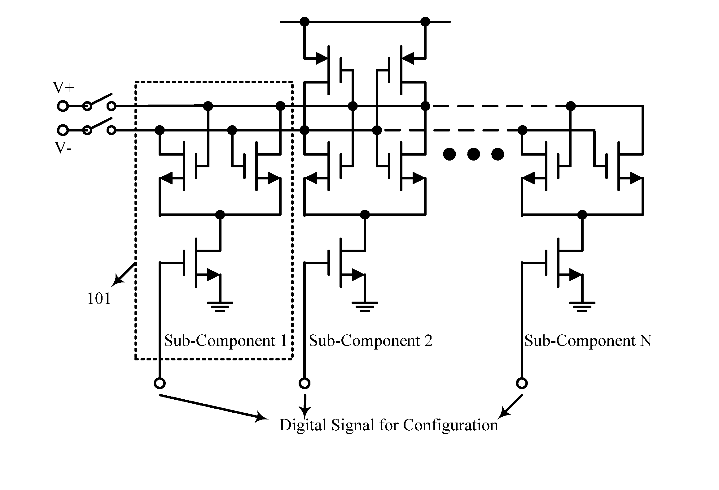
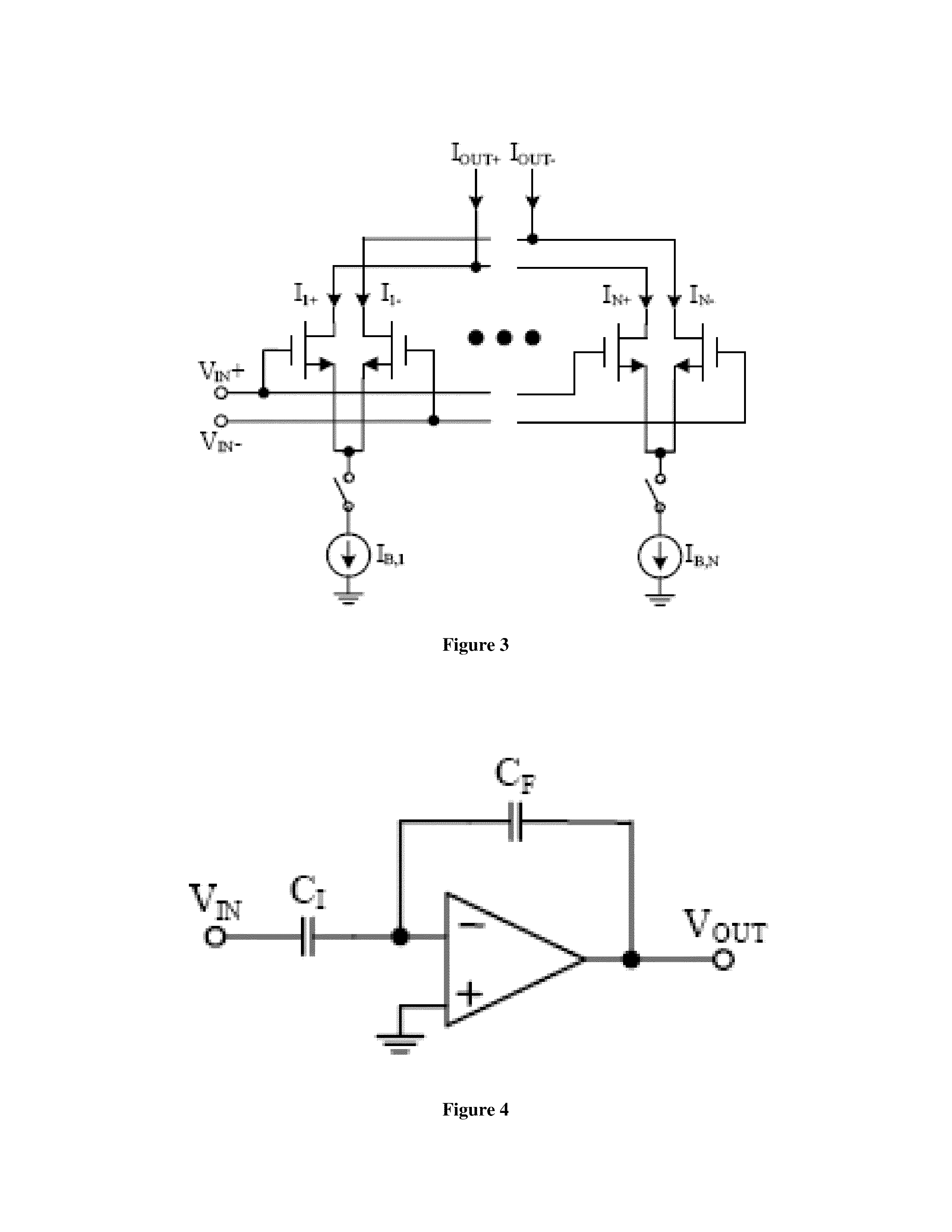
[0070]Two analog design examples (i.e., a differential transistor pair and a switched-capacitor amplifier) are used in this embodiment to illustrate the basic concept of the proposed adaptive post-silicon tuning. The following two circuit examples rely on transistor matching and capacitor matching, respectively. It should be noted, however, that the proposed post-silicon tuning methodology can be applied to many other analog applications where device matching is critical.

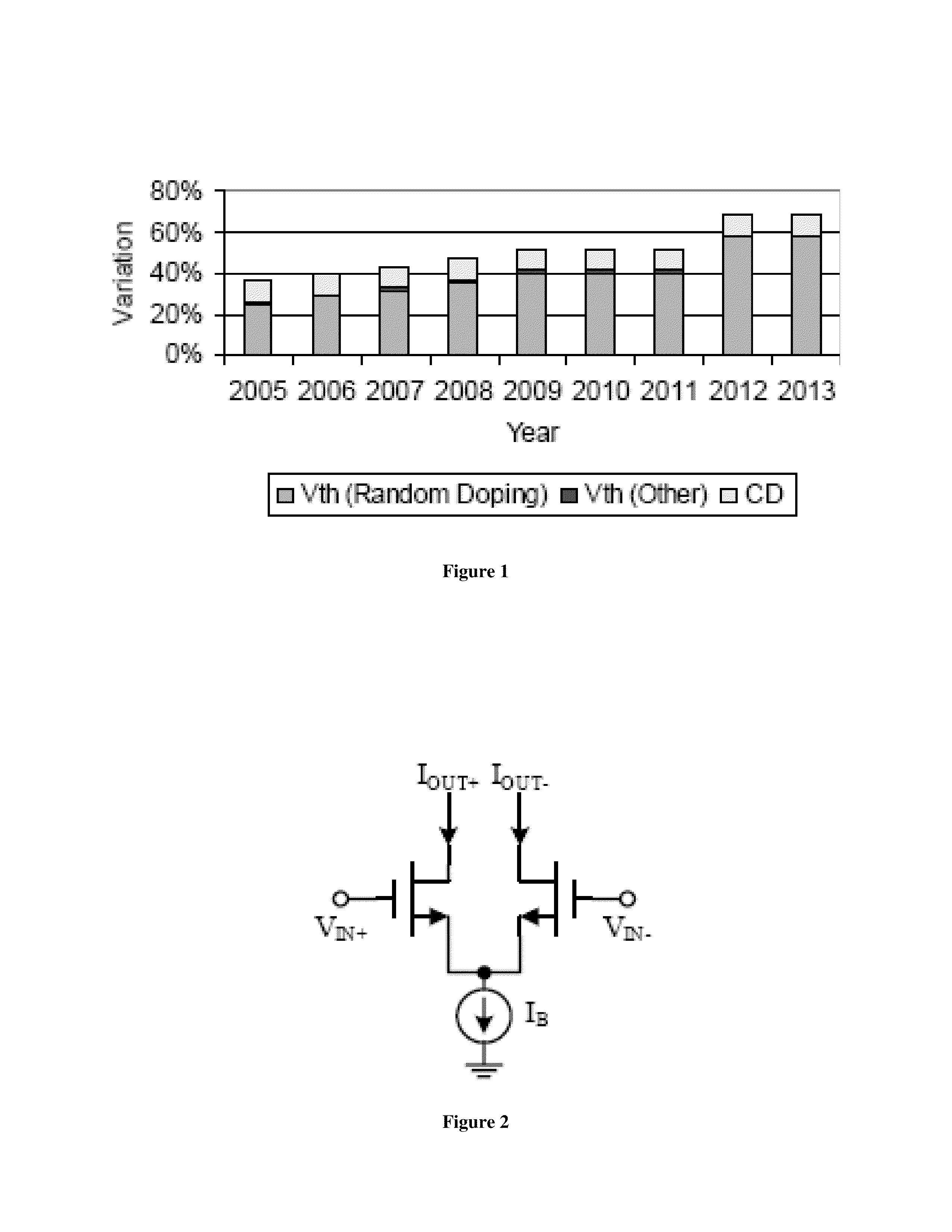
[0071]Shown in FIG. 2 is the simplified circuit schematic of a traditional differential transistor pair (see Background reference [23]). It utilizes the symmetric topology to make the performance insensitive to inter-die variations. However, random device mismatches make the circuit symmetric and, hence, introduce offset voltage. In general, the transistors of a differential pair must be sufficiently large so that the offset voltage can be minimized.

[0072]An...

second embodiment

Method for Tuning Circuit Design

[0183]This embodiment discloses a method for a method for use with a circuit, the circuit comprising first and second components, said first and second components disposed on a common semiconductor substrate, said first and second components originating from the same semiconductor-fabrication process, each said component defining an operational value capable of being measured post-fabrication, each said component comprising a respective number of respective sub-components, each of said sub-components contributing a fractional portion of the operational value of the respective component, each of said sub-components disposed to be operational or non-operational under configurable control, the operational value being a consequence of the aggregate of the sub-components, the method comprising the steps of: carrying out a plurality of post-fabrication measurements of the operational value for the first component, each post-fabrication measurement carried o...

third embodiment

Method of Use with an Analog Circuit

[0196]This embodiment discloses a method for use with a circuit, the circuit comprising a component, said component disposed on a semiconductor substrate, said component defining an operational value capable of being measured post-fabrication, said component comprising respective sub-components, said respective sub-components originating from the same semiconductor-fabrication process, each of said sub-components contributing a fractional portion of the operational value of said component, each of said sub-components disposed to be operational or non-operational under configurable control, the operational value being a consequence of the aggregate of the sub-components, the method comprising the steps of: carrying out a plurality of post-fabrication measurements of the operational value for said component; selecting a subset of said sub-components for said component, based upon its measured operational values; and configuring said selected sub-com...


PUM


Abstract

The invention discloses a method for tuning nano-scale analog-circuit designs in order to reduce random-device mismatches and optimize said design, where nano-scale devices potentially have large-scale process variations. The method includes providing a tunable circuit topology, wherein each nano-scale device comprises a single component or comprises multiple parallel components. Each component is decomposed into multiple discrete sub-components, wherein each said sub-component either operates in parallel with other like components to effectively operate like one bigger component. The sub-components are subjected to a dynamic-programming process to adaptively select the sub-components to be kept operational, while configuring the nonselected sub-components to be nonoperational, based on the measurement of at least one operational parameter.

Description

CROSS-REFERENCE TO RELATED APPLICATIONS[0001]This application claims priority from U.S. application No. 60 / 976,682, filed Oct. 1, 2007, which application is incorporated herein by references for all purposes.BACKGROUND[0002]1. Background Discussion[0003]NOTE: Some of the references referred in this subsection, using the reference number contained in the square brackets [ ], are listed to in the next subsection.[0004]The continued scaling of CMOS technologies has brought about increasing uncertainties in process parameters to the point for which it is difficult to create reliable, robust design over all process variations. As integrated circuits continue to aggressively scale to smaller feature size (e.g., 65 nm, 45 nm, etc.), it is extremely difficult, if not impossible, to reliably manufacture circuits while achieving high product yield (or equivalently, low manufacturing cost). Traditional robust IC design methodologies (e.g., corner-based design and statistical design) attempt to...

Claims


Application Information

Patent Timeline
Patent Type & Authority Patents(United States)
IPC IPC(8): G06F17/50
CPCH03J5/244H03J2200/10
Inventor PILEGGI, LAWRENCE T.LI, XIN
Owner CARNEGIE MELLON UNIV
Why Eureka
Try Eureka