

Pixel circuit having flip-flop with inverter and feedback transistor, electro-optical device having said pixel circuit, and electronic apparatus having said electro-optical device
a pixel circuit and feedback transistor technology, applied in the field of pixel circuits, can solve the problems of easy generation of non-uniform display, easy change of maintained voltage caused by leak current, and easy generation of maintained voltage, so as to improve display quality of small-size electronic devices, high reliability, and high accuracy
- Summary
- Abstract
- Description
- Claims
- Application Information
AI Technical Summary
Benefits of technology
Problems solved by technology
Method used
Image

Examples
first embodiment
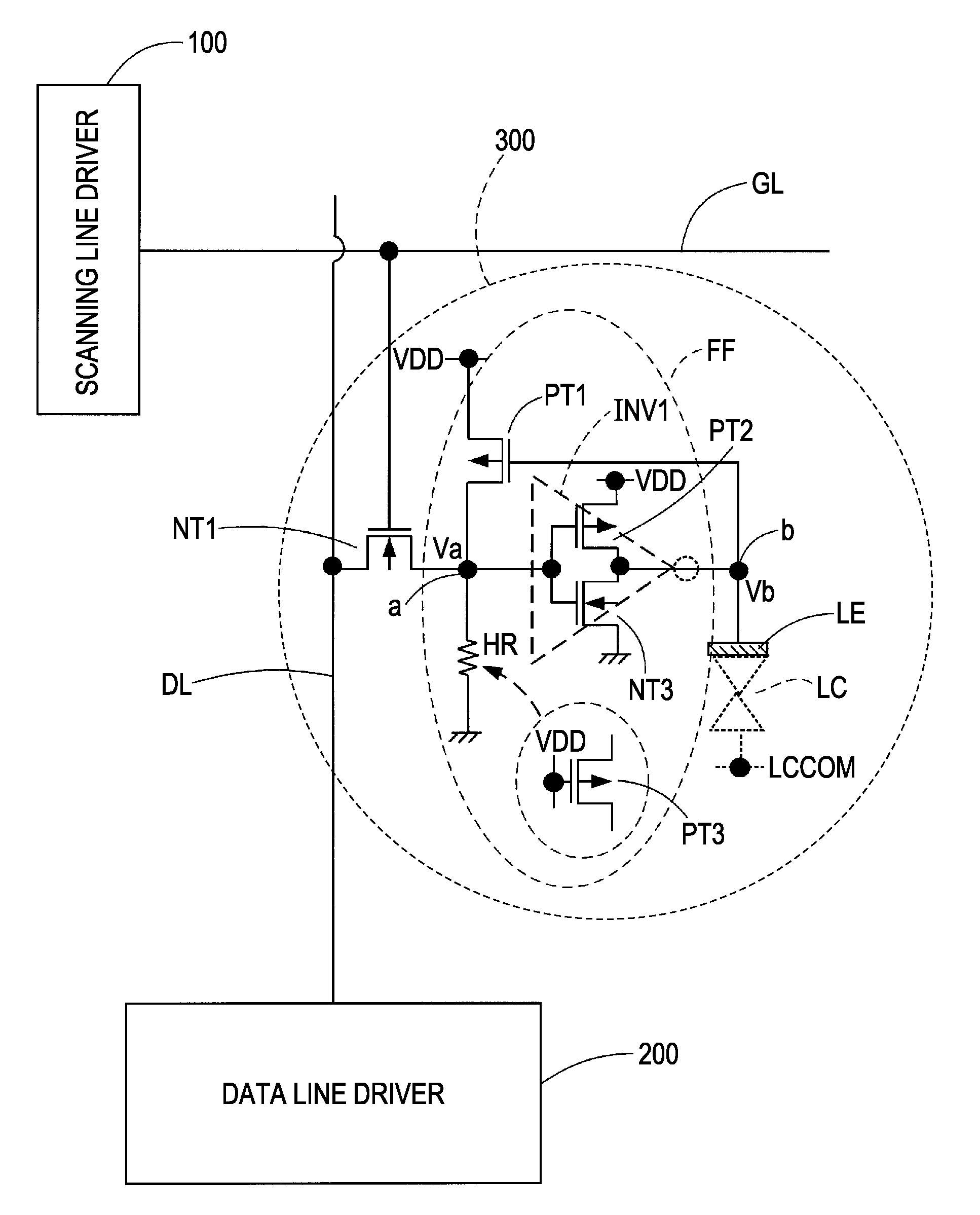
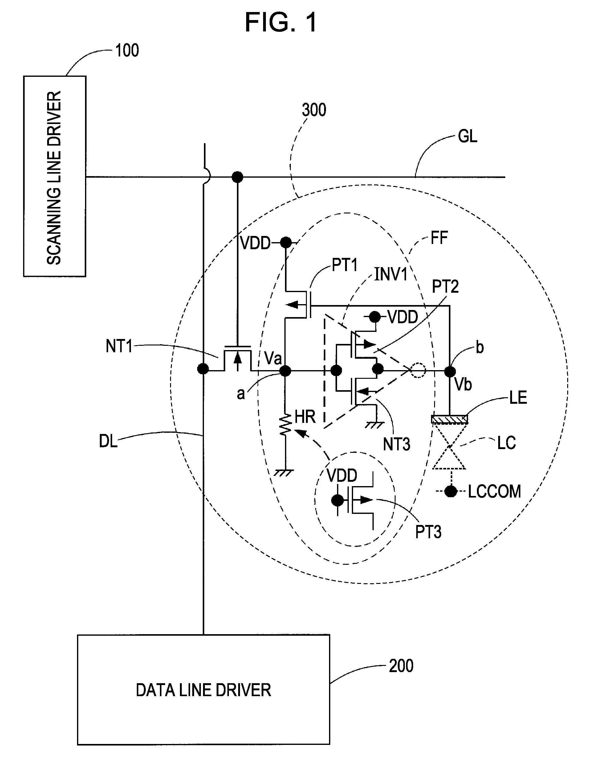
[0057]FIG. 1 is a circuit diagram showing an example of the configuration of a pixel circuit according to an embodiment of the invention. As shown in the figure, the pixel circuit 300 is disposed in correspondence with an intersection of a scanning line GL and a data line DL. The scanning line GL is driven by a scanning line driver 100, and the data line DL is driven by a data line driver 200.
[0058]The pixel circuit 300, for example, includes a pixel transistor NT1 that is formed by an NMOS transistor (n-channel insulated gate-type field effect transistor regardless of the type of an insulation film), a flip-flop FF, and a pixel electrode LE (electrode for applying a voltage to a liquid crystal LC).
[0059]The flip-flop FF includes a CMOS inverter INV1 that operates between the high-level power source voltage VDD and the low-level power source voltage GND and a feedback transistor PT1 that is formed of a PMOS transistor. The CMOS inverter INV1 and the feedback transistor PT1 form a po...
second embodiment
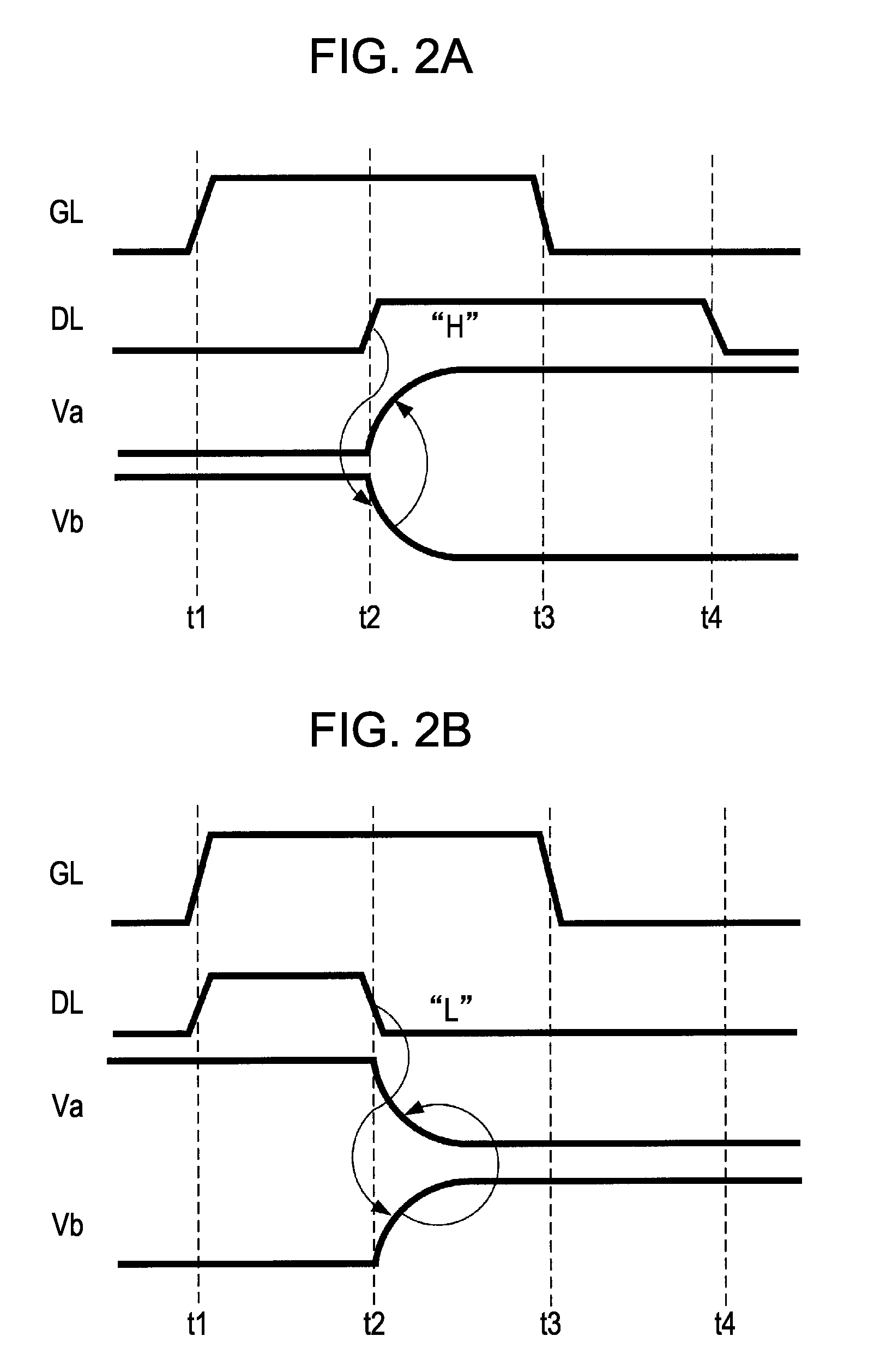
[0078]In a second embodiment of the invention, a countermeasure for a change in the writing voltage due to the feed-through voltage of the pixel transistor will be described. FIGS. 4A to 4C are diagrams for describing adjustment of the threshold voltage of the CMOS inverter as a countermeasure for the change in the writing voltage due to the feed-through voltage of the pixel transistor.
[0079]In FIG. 4A, it is assumed that “1” is written into the pixel circuit. When a writing operation is completed and the voltage of the scanning line GL changes from H to L, a push-down voltage (feed-through voltage: −ΔV) is generated due to parasitic capacitance Cgd between the gate and drain of the pixel transistor (NMOS transistor) NT1. Accordingly, the electric potential of point “a” becomes (VDD−ΔV). FIG. 4C shows transfer characteristics of the CMOS inverter INV1. As denoted by a dotted line in FIG. 4C, for example, in a case where the threshold voltage is set to VDD / 2, when the absolute value ...
third embodiment
[0082]FIGS. 5A and 5B are diagrams showing an improved example for a case where data “0” is written into the pixel circuit that maintains data “1”.
[0083]As shown in FIG. 5A, data “1” (=VDD) is maintained at the holding node (point a) of the pixel circuit. In this state, as shown in FIG. 5B, a case where data “0” (=GND) is written into the pixel circuit will be considered.
[0084]In this case, when the scanning line GL has a selection electric potential (H), the pixel transistor NT1 is turned on. Accordingly, an on-current Ionn1 flows from the holding node (point a) to the data line DL. When the on-current Ionn1 of the pixel transistor NT1 is larger than the on-current Ionp1 of the feedback transistor PT1, the voltage level of the holding node (point a) transits from the H level to the L level. Accordingly, data “0” can be written.
[0085]Thus, in order to perform a writing operation assuredly, the characteristics (design values such as the sizes) of the pixel transistor NT1 and the feed...
PUM
 Abstract
Description
Claims
Application Information