Coating and developing apparatus, substrate processing method, and storage medium

a technology of which is applied in the direction of photomechanical treatment, instruments, and photosensitive materials, can solve the problems of reducing the efficiency of substrate transferring, occupying less space for substrate inspection units in process blocks, and disadvantageous space and transfer channels, etc., so as to reduce the space occupied by coating and developing apparatus, the effect of favorable contour

Active Publication Date: 2011-06-07
TOKYO ELECTRON LTD
View PDF17 Cites 0 Cited by
  • Summary
  • Abstract
  • Description
  • Claims
  • Application Information

AI Technical Summary

Benefits of technology

[0012]The present invention has been made in view of the foregoing circumstances. The object of the present invention is to provide a coating and developing apparatus which requires a smaller occupation space even when it incorporates a substrate inspection unit, while eliminating a disadvantageous layout. Another object of the present invention is to provide a substrate processing method and a storage medium storing a program for executing the substrate processing method, which are capable of enhancing a throughput when the coating and developing apparatus is operated to inspect a processed substrate.
[0029]According to the present invention, the substrate inspection unit is incorporated in one of the coating film forming part and the developing part that are vertically arranged. According to another invention, the substrate inspection part including the substrate inspection unit is vertically arranged on the coating film forming part and the developing part. In either of the inventions, the outward protrusion of the substrate inspection unit from the body of the coating and developing apparatus can be avoided. As a result, the coating and developing apparatus can have a favorable contour, and a space occupied by the coating and developing apparatus can be reduced.

Problems solved by technology

This structure complicates the transfer channel of the substrate, which results in a degraded substrate transferring efficiency.
Further, since the interface block P3 accommodates a buffer cassette for absorbing a difference in processing speeds of the interface block P3 and the exposure apparatus, and a temperature adjusting unit for precisely setting a temperature of the substrate at a temperature of the exposure apparatus, there is not an enough space for the substrate inspection unit in the process block.
Alternatively, disposition of the substrate inspection unit 13 in the process block P2 is disadvantageous in terms of space and transfer channel.
Thus, when the coating and developing apparatus together with the substrate inspection unit is installed in a clean room, such an installation is inefficient in the utilization of space, whereby there arises a problem regarding arrangement of a peripheral equipment and securement of a maintenance space.
In particular, when a larger substrate, e.g. a substrate such as a semiconductor wafer (referred to as “wafer” below) having a diameter not less than 12 inches is processed, the substrate inspection unit 13 is necessarily enlarged, which makes the problem more serious.
However, this layout requires a larger space for installation including a layout of the process block.
In addition, since a substrate transfer mechanism disposed on the inspecting block takes charge both of a transferring operation of a substrate between the carrier block and the process block and a transferring operation of a substrate to the inspection unit, the transfer mechanism bears an increased burden.

Method used


Image

  • Coating and developing apparatus, substrate processing method, and storage medium
  • Coating and developing apparatus, substrate processing method, and storage medium
  • Coating and developing apparatus, substrate processing method, and storage medium

Examples


first embodiment

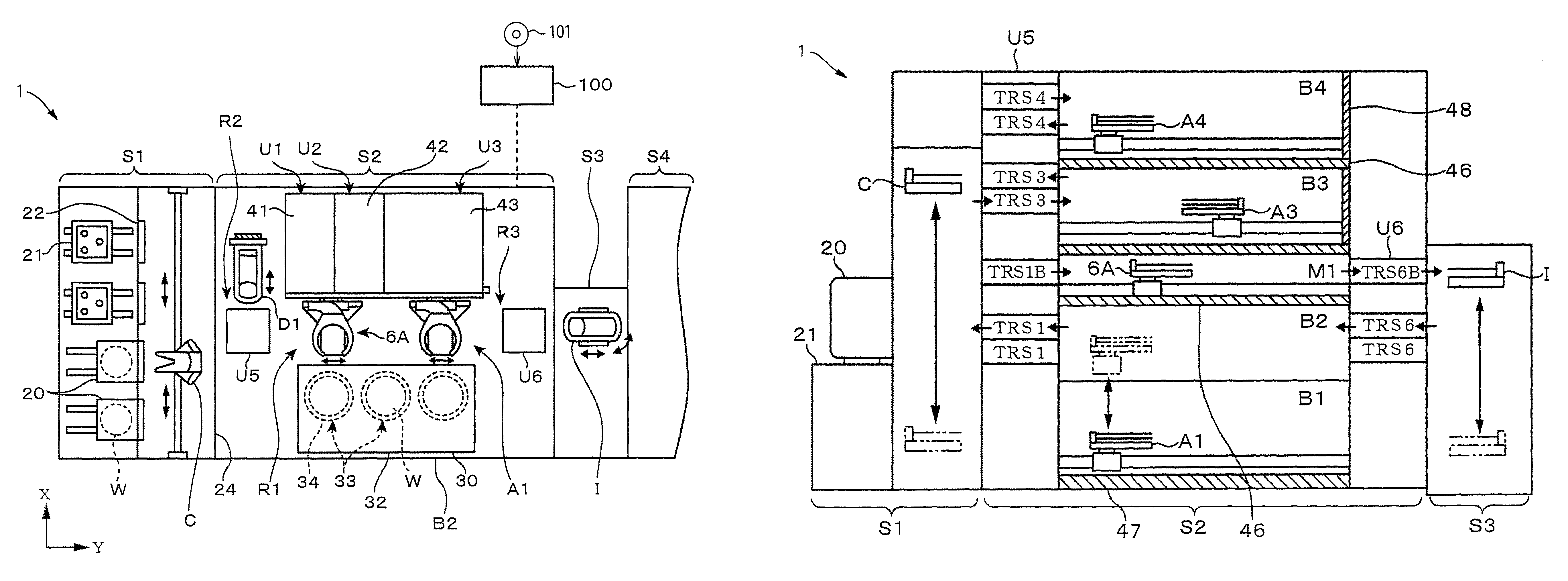
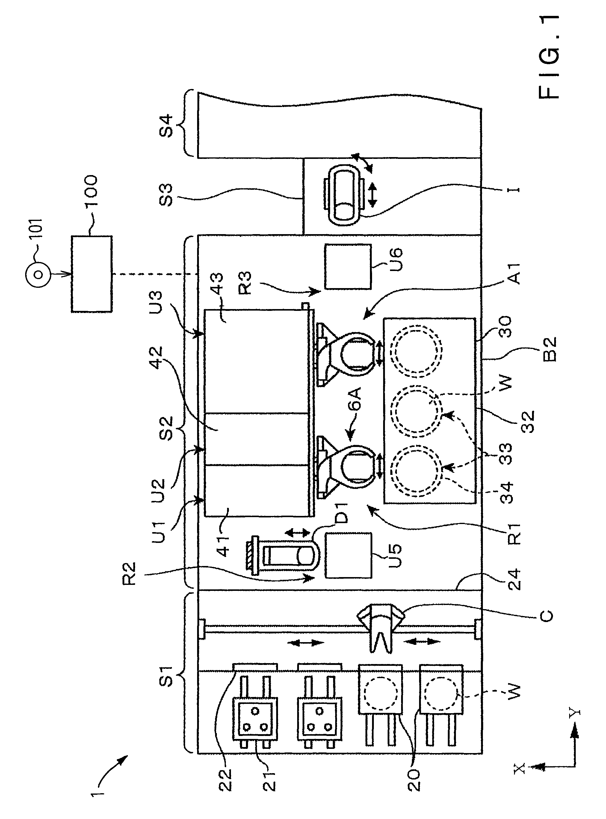
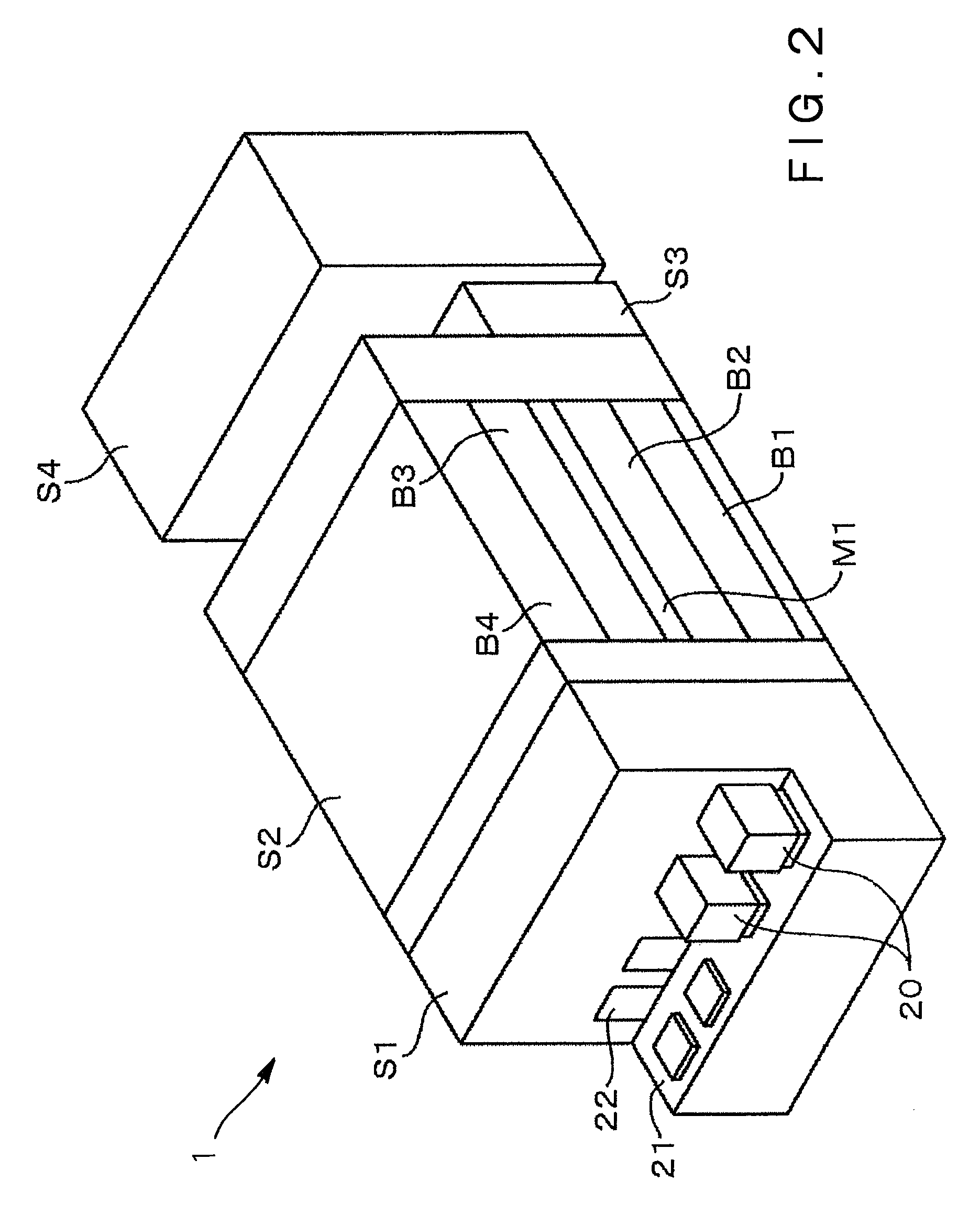
[0045]A first embodiment is described with reference to FIGS. 1 to 5. FIGS. 1 and 2 show a system in which an exposure apparatus is connected to a developing apparatus. The coating and developing apparatus 1 includes a carrier block (carrier area) S1 on which a carrier 20 capable of hermetically containing a plurality of substrates (e.g., thirteen wafers W), a process block (process area) S2 having a plurality of, e.g., four parts (four sections) B1 to B4 and a direct transfer part (direct transfer section) M1 arranged along a longitudinal direction of the overall system, and an interface block (interface area) S3. An exposure apparatus S4 is connected to the interface block S3.

[0046]The carrier block S1 accommodates a table 21 on which a plurality of carriers 20 can be placed, opening and closing parts 22 formed in a wall surface ahead the table 21, and a conveying arm (transfer mechanism for the carrier block) C capable of taking out the wafer W from the carrier 20 through the ope...

second embodiment

[0092]A coating and developing apparatus 1 in this embodiment has substantially the same structure as that of the coating and developing apparatus in the However, the coating and developing apparatus 1 in this embodiment does not have the direct transfer part M1, the transfer unit TRS1B of the tier-like unit group U5, and the transfer unit TRS6B of the tier-like unit group U6. FIG. 12 is a cross-sectional view of a substrate inspection part B5 of the coating and developing apparatus 1 in this embodiment. As shown in FIG. 12, similar to DEV layers B1 and B2, an area of the substrate inspection part B5 on a side of an interface block B3 provides a wafer transfer area R3. A tier-like unit group U6 having a transfer unit TRS7 is arranged in the area R3 at a height position facing the substrate inspection part B5 of the tier-like unit group U6. A transfer arm D2 having, e.g., the same structure as that of a transfer arm D1 is disposed in the wafer transfer area R3. The transfer arm D2 c...


PUM

PropertyMeasurementUnit
diameteraaaaaaaaaa
heightaaaaaaaaaa
widthaaaaaaaaaa

Abstract

A coating and developing apparatus is provided which requires a smaller occupation space even when it incorporates a substrate inspection unit, while eliminating a disadvantageous layout. A coating film forming part B3 including a plurality of process units and transfer mechanisms A3 and A4, and a developing part B1 including a plurality of process units 31 and a transfer mechanism A1 are vertically arranged in a process block S2. There are disposed in the process block S2 on a side of a carrier block S1, a plurality of vertically arranged transfer units TRS for transferring a substrate W between the same and transfer mechanisms for the respective parts, and a vertically movable transfer mechanism D1 for the transfer unit for transferring a substrate between these transfer units. At least one of the coating film forming part and the developing part includes a substrate inspection unit 43 for inspecting a substrate transferred by the transfer mechanism for the corresponding part.

Description

CROSS REFERENCE TO RELATED APPLICATIONS[0001]This application is based upon and claims the benefit of priority from the prior Japanese Patent Application No. 2006-112704 filed on Apr. 14, 2006, the entire contents of which are incorporated herein by reference.BACKGROUND OF THE INVENTION[0002]1. Field of the Invention[0003]The present invention relates to a coating and developing apparatus for coating a substrate such as a semiconductor wafer or an LCD substrate (glass substrate for a liquid crystal display panel) with a resist liquid and developing the substrate after exposure thereof, a substrate processing method, and a storage medium storing a program for executing the substrate processing method.[0004]2. Description of Related Art[0005]One of the processes for manufacturing a semiconductor device and an LCD substrate includes a series of steps in which a resist film is formed on a substrate, then the resist film is exposed with the use of a photomask, and thereafter the resist f...

Claims


Application Information

Patent Timeline
Patent Type & Authority Patents(United States)
IPC IPC(8): G03D5/04
CPCH01L21/67745H01L21/67178G03F1/60G03F1/84H01L21/02027H01L21/0274G03F7/16H01L21/02002H01L21/02019
Inventor MATSUOKA, NOBUAKIHAYASHIDA, YASUSHIHAYASHI, SHINICHI
Owner TOKYO ELECTRON LTD
Why Eureka
Try Eureka