Method for fabricating nanoscale thermoelectric device

a thermoelectric device and nano-scale technology, applied in thermoelectric device manufacturing/treatment, material nanotechnology, electrical apparatus, etc., can solve the problems of increasing the working clock of single-core microprocessor, increasing heat dissipation cost without increasing performance equally, and miniaturizing high-performance chips, etc., to achieve high thermoelectric conversion efficiency

Inactive Publication Date: 2011-06-14
NAT CHIAO TUNG UNIV
View PDF17 Cites 21 Cited by
  • Summary
  • Abstract
  • Description
  • Claims
  • Application Information

AI Technical Summary

Benefits of technology

The primary objective of the present invention is to provide a method for fabricating a nanoscale thermoelectric device, whereby a high thermoelectric conversion efficiency element having P-type and N-type nanoscale wires can be fabricated.
Further objective of the present invention is to provide a method for fabricating a nanoscale thermoelectric device, whereby the compositions of the alloys for nanoscale wires can be precisely controlled.

Problems solved by technology

Under the current packaging design, increasing the working clock of the single-core microprocessor will generate much more heat and obviously increase the heat-dissipation cost without increasing the performance equally.
However, the miniaturized, high-speed, and high performance chips bear the problem of heat dissipation.
However, the thermoelectric element has a poor thermoelectric conversion efficiency because it has larger dimensions.
However, the thermoelectric element also has a poor thermoelectric conversion efficiency because it only uses a single type of element.
The prior art is not suitable to fabricate nanoscale wires having a melting point close to or higher than the melting point of aluminum.
However, the equipment is expensive, and the fabrication process is complicated, and the environmental control is rigid.
Therefore, the prior art is not suitable for mass production.
However, electrodeposition is apt to have impurities and is hard to control alloy composition, particularly the composition of a more than ternary alloy.

Method used


Image

  • Method for fabricating nanoscale thermoelectric device
  • Method for fabricating nanoscale thermoelectric device
  • Method for fabricating nanoscale thermoelectric device

Examples


Embodiment Construction

IC and semiconductor fabrication still dominates the science and technology industry in Taiwan. As the current trend of 3C products is toward cheapness and slimness, heat dissipation has become the biggest challenge in the field concerned. Therefore, the market of high-performance heat-dissipation elements will expand considerably with the stable growth of computer and optoelectronic industries. Below is described in detail a method for fabricating a high-efficiency nanoscale thermoelectric device.

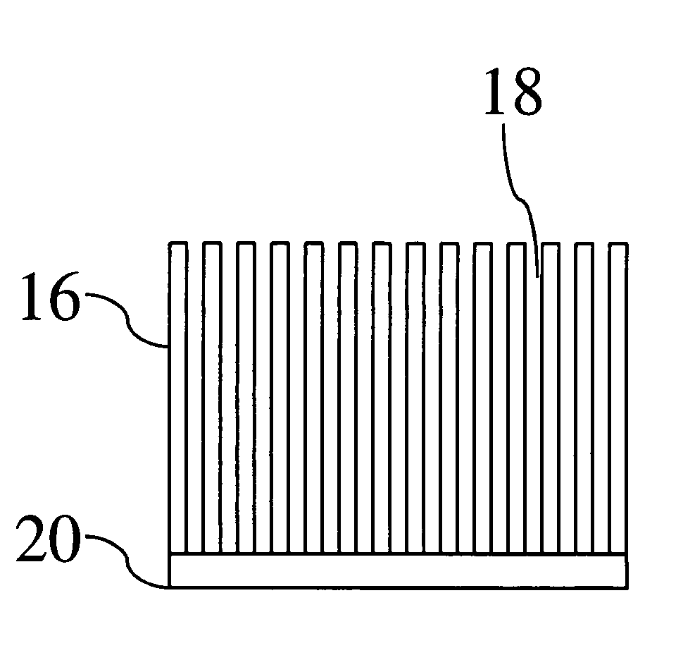
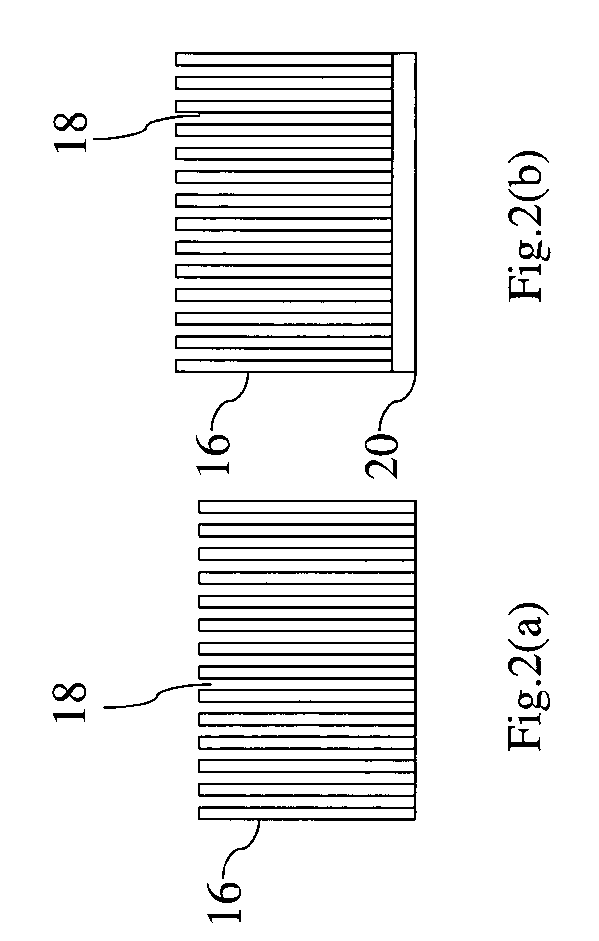
Refer to from FIG. 2.(a) to FIG. 2(d) diagrams schematically showing the steps of fabricating a semiconductor nanoscale wire array according to one embodiment of the present invention. As shown in FIG. 2(a), a template 16 having a group of nanoscale pores 18 is provided firstly. The template 16 may be made of alumina, titanium oxide, silicon dioxide, opal or zeolite. The nanoscale pores 18 may have an appearance of a triangular, rectangular or circular array, and the array has an area of a...


PUM

PropertyMeasurementUnit
diameteraaaaaaaaaa
diameteraaaaaaaaaa
lengthaaaaaaaaaa

Abstract

The present invention discloses a method for fabricating a nanoscale thermoelectric device, which comprises steps: providing at least one template having a group of nanoscale pores; forming a substrate on the bottom of the template; injecting a molten semiconductor material into the nanoscale pores to form a group of semiconductor nanoscale wires; removing the substrate to obtain a semiconductor nanoscale wire array; and using metallic conductors to cascade at least two semiconductor nanoscale wire arrays to form a thermoelectric device having a higher thermoelectric conversion efficiency.

Description

BACKGROUND OF THE INVENTION1. Field of the InventionThe present invention relates to a fabrication method, particularly to a method for fabricating a nanoscale thermoelectric device.2. Description of the Related ArtFew years ago, Intel Company announced that the dual-core microprocessor would replace the single-core microprocessor because the development of the existing single-core microprocessor had reached its ultimate. Under the current packaging design, increasing the working clock of the single-core microprocessor will generate much more heat and obviously increase the heat-dissipation cost without increasing the performance equally. Therefore, a 65-nm dual-core process is a necessary approach to promote the performance of microprocessors. However, the miniaturized, high-speed, and high performance chips bear the problem of heat dissipation. If the problem of heat dissipation cannot be resolved, many key elements in the fields of communication, optoelectronics, power, aerospace...

Claims


Application Information

Patent Timeline
Patent Type & Authority Patents(United States)
IPC IPC(8): H01L21/00
CPCB82Y10/00H01L35/34H01L35/32B82Y30/00Y10S977/70Y10S977/762Y10S977/781Y10S977/888Y10S977/833H10N10/01H10N10/17
Inventor CHAO, CHUEN-GUANGCHEN, JUNG-HSUANYANG, TA-WEI
Owner NAT CHIAO TUNG UNIV
Why Eureka
Try Eureka