Magnetoresistance effect device and magnetism sensor using the same

a technology of magnetism sensor and effect device, which is applied in the direction of magnetic bodies, instruments, transportation and packaging, etc., can solve the problems of inability to use the main materials in the semiconductor technology to incorporate into the line of semiconductor fabrication, disadvantages of material incorporation, and inability to industrialize, and achieves the effect of high sensitivity to magnetic field, excellent characteristics, and simple process

Inactive Publication Date: 2011-06-21
NAT INST OF ADVANCED IND SCI & TECH
View PDF17 Cites 3 Cited by
  • Summary
  • Abstract
  • Description
  • Claims
  • Application Information

AI Technical Summary

Benefits of technology

[0024]As described above, the magneto-resistance effect device of the present invention exhibits a high magneto-resistance effect at room temperature, is highly sensible to a magnetic field and can be produced through a simple process in spite of the fact that the fundamental structure thereof is a very simple structure having a multiplicity of metal particles dispersed on a semiconductor substrate.

Problems solved by technology

For example, materials that cannot be incorporated into a line of semiconductor fabrication using the main materials in the semiconductor technologies, such as silicon and gallium arsenic, or materials requiring great labor for the incorporation are disadvantageous from the standpoint of the industrialization.
In most cases, materials containing magnetic metal elements, such as iron, chromium and cobalt, are not suitable for the industrialization.
It goes without saying that it is difficult for the devices to be used as actual magneto-resistance effect devices insofar as the characteristics of the devices cannot be manifested at room temperature.
As is clear from Table 1, the materials exhibiting high magneto-resistance effect, such as materials f, g and h in Table 1, have drawbacks that these can only operate at low temperatures and that these require an extremely high magnetic field.
As described above, the conventional magneto-resistance devices could only operate at low temperatures or required an extremely high magnetic field.

Method used


Image

  • Magnetoresistance effect device and magnetism sensor using the same
  • Magnetoresistance effect device and magnetism sensor using the same
  • Magnetoresistance effect device and magnetism sensor using the same

Examples


Embodiment Construction

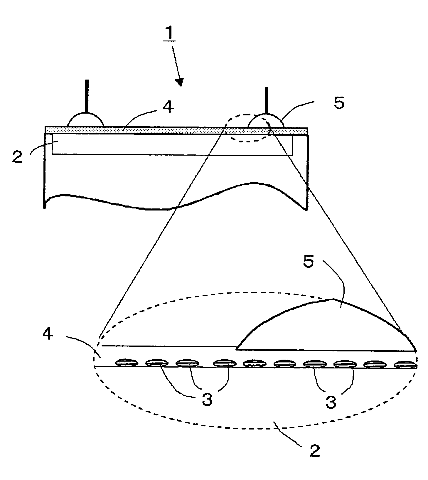
[0047]An embodiment of the magneto-resistance effect device will first be described and an embodiment of the magnetic field sensor using the magneto-resistance effect device will then be described.

[0048]A magneto-resistance effect device 1 of the present invention has a structure shown in FIG. 13, in which a semiconductor substrate 2 has a multiplicity of metal micro-particles 3 dispersed thereon and covered by an ultra-thin, semiconductor or half-metal, cap layer 4, and has as an operation principle a magneto-resistance effect that varies the resistance of the granular thin layer through application of a magnetic field.

[0049]The magneto-resistance effect device 1 exhibits a magneto-resistance effect one order higher than that obtained from an existing device even in a magnetic field of 100 Oe or less. Varying the voltage applied between the two electrodes 5 shown in FIG. 13 enables the magneto-resistance ratio of the device to be adjusted to conform to the magnetic field intensity....


PUM

PropertyMeasurementUnit
sizeaaaaaaaaaa
sizeaaaaaaaaaa
thicknessaaaaaaaaaa

Abstract

A magneto-resistance effect device (1) includes a semiconductor region (2) having a surface provided with a plurality of isolated metal micro-particles (3) of not more than 100 μm disposed at intervals of not more than 1 μm, a semiconductor or half-metal cap layer (4) for covering the semiconductor region and a plurality of electrodes (5) disposed on a surface of the cap layer and separated from each other. The device exhibits a high magneto-resistance effect at room temperature, is highly sensible to a magnetic field and can be produced through a simple manufacturing process. The device is formed of a magneto-resistant material easy to match a semiconductor fabrication process. A magnetic field sensor using the device (1) has various excellent characteristics.

Description

TECHNICAL FIELD[0001]This invention relates to a magneto-resistance effect device comprising a semiconductor and micro-particles of metal and to a magnetic field sensor using the magneto-resistance effect device. Particularly, the invention relates to a magneto-resistance effect device using a magnetic filed to control a large resistance variation resulting from the electron avalanche effect and to a magnetic field sensor using the magneto-resistance effect device.BACKGROUND ART[0002]In recent years, studies have been actively made on magnetic field sensor devices being made highly sensitive, developments of magnetic memory devices, etc., utilizing a so-called magneto-resistance effect that is the effect of varying resistance with a change in external magnetic field. The competition among researchers and developers for these devices falling in one of the advanced technical fields that support the information technology developing at ever-progressing speed is being intensified.[0003]...

Claims


Application Information

Patent Timeline
Patent Type & Authority Patents(United States)
IPC IPC(8): H01L29/82G01R33/09H01F10/193H01L43/08
CPCB82Y25/00G01R33/09G01R33/093H01F10/1936H01L43/08G01R33/1269Y10T428/12465H01L27/222H10B61/00H10N50/10
Inventor AKINAGA, HIROYUKIOSHIMAMIZUGUCHI, MASAKI
Owner NAT INST OF ADVANCED IND SCI & TECH
Why Eureka
Try Eureka