Method and system for electromigration analysis on signal wiring

a signal wiring and electromigration analysis technology, applied in error detection/correction, program control, instruments, etc., can solve the problem of relatively pessimistic time parameters used in timing analysis, and achieve the effect of improving wiring quality

Active Publication Date: 2011-06-28
SIEMENS PROD LIFECYCLE MANAGEMENT SOFTWARE INC
View PDF8 Cites 13 Cited by
  • Summary
  • Abstract
  • Description
  • Claims
  • Application Information

AI Technical Summary

Benefits of technology

[0011]The objects of the invention are to provide an improved method and an improved system for electromigration analysis on signal wiring in such a way as to maintain topological information during electromigration analysis to improve wiring quality.
[0014]No extra driver characterization is necessary, thus simplifying the modeling. Individual failing segments and / or vias can be easily identified. A typical noise analysis considers crosstalk effects between adjacent lines and uses high-speed driver with high voltages and high current. A typical timing analysis uses relatively pessimistic time parameters at lower voltages, usually using relatively slow drivers. However, timing analysis can also be done with high-speed drivers. Favorably, at least the slew rate and probably a load capacity of one or more load cell can be taken from the timing analysis run of the complete chip or from a run of a part of the chip using detailed wire models. Preferably, cycle time and switching factor used for the driver voltage signals can be determined from the same timing run. Cycle time is characterized by the frequency extracted from a design database for the chip considered. Generally, the cycle time is the reciprocal value of the clock frequency. The switching factor can be defined or calculated for specific functions. The switching factor, generally, describes how often a signal switches per clock cycle. The switching factor for a clock signal usually is defined as 1, whereas the switching factor for a data signal is below 1, e.g. 0.2 or the like. The voltage levels are preferably extracted from a design database used in the layout of the chip.
[0016]Preferably, each segment of an interconnection of a net can be annotated by its layer number, wire width and / or coordinates in the net generated as layout extraction data. Thus, detailed and accurate geometrical data are available and allow estimating the local thermal load on the interconnections caused by a current flow. If a good thermal conduction and / or a good removal of excess heat is possible, the current density limit can be higher than in a case where surrounding elements of the electric circuit thermally isolate the segment and / or via or even add thermal load to the segment and / or via. The accuracy of the electromigration analysis can be increased.
[0017]By setting an individual maximum effective current density limit for each segment and / or via between metal layers of the interconnections, the accuracy of the analysis can be increased further. Typically, the electric conductors forming vias are of standard size and thickness defined by the fabrication technology process used for preparing the integrated electric circuit. Therefore, the current density limits of the vias are dependent mainly on the via position. Preferably, each via of a redundant array can be handled individually. However it is possible to handle all vias of a redundant array at once as a complete array of vias. A redundant array of vias is to be understood as two or more parallel vias establishing an electric contact between a segment of a specific net in a first metal layer to a segment of the same net in another metal layer. This provides a safe electrical contact between segments running in different metal layers as during processing a chip there is a finite probability that a via cannot be opened and is thus electrically insulating.
[0021]In a further advantageous method step the accuracy of the analysis can be increased if a DC component in the measured current density values can be eliminated. This can be done by reading the value at the end of the train of voltage pulses sent by the driver cell. For example, if the pulse train consists of ten pulses, the reading of the value can be done at the tenth pulse. By doing so, the measured current density values are automatically averaged which in turn eliminates the DC component.

Problems solved by technology

A typical timing analysis uses relatively pessimistic time parameters at lower voltages, usually using relatively slow drivers.

Method used


Image

  • Method and system for electromigration analysis on signal wiring
  • Method and system for electromigration analysis on signal wiring
  • Method and system for electromigration analysis on signal wiring

Examples


Embodiment Construction

[0040]The drawings are merely schematic representations, not intended to portray specific parameters of the invention. Moreover, the drawings are intended to depict only typical embodiments of the invention and therefore should not be considered as limiting the scope of the invention. In the drawings, like elements are referred to with equal reference numerals.

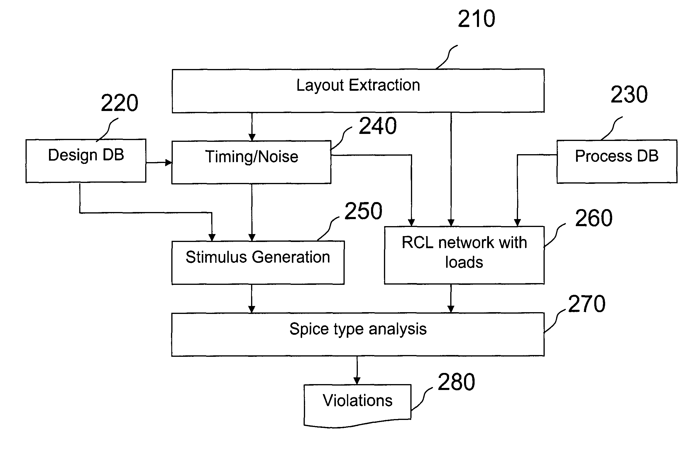
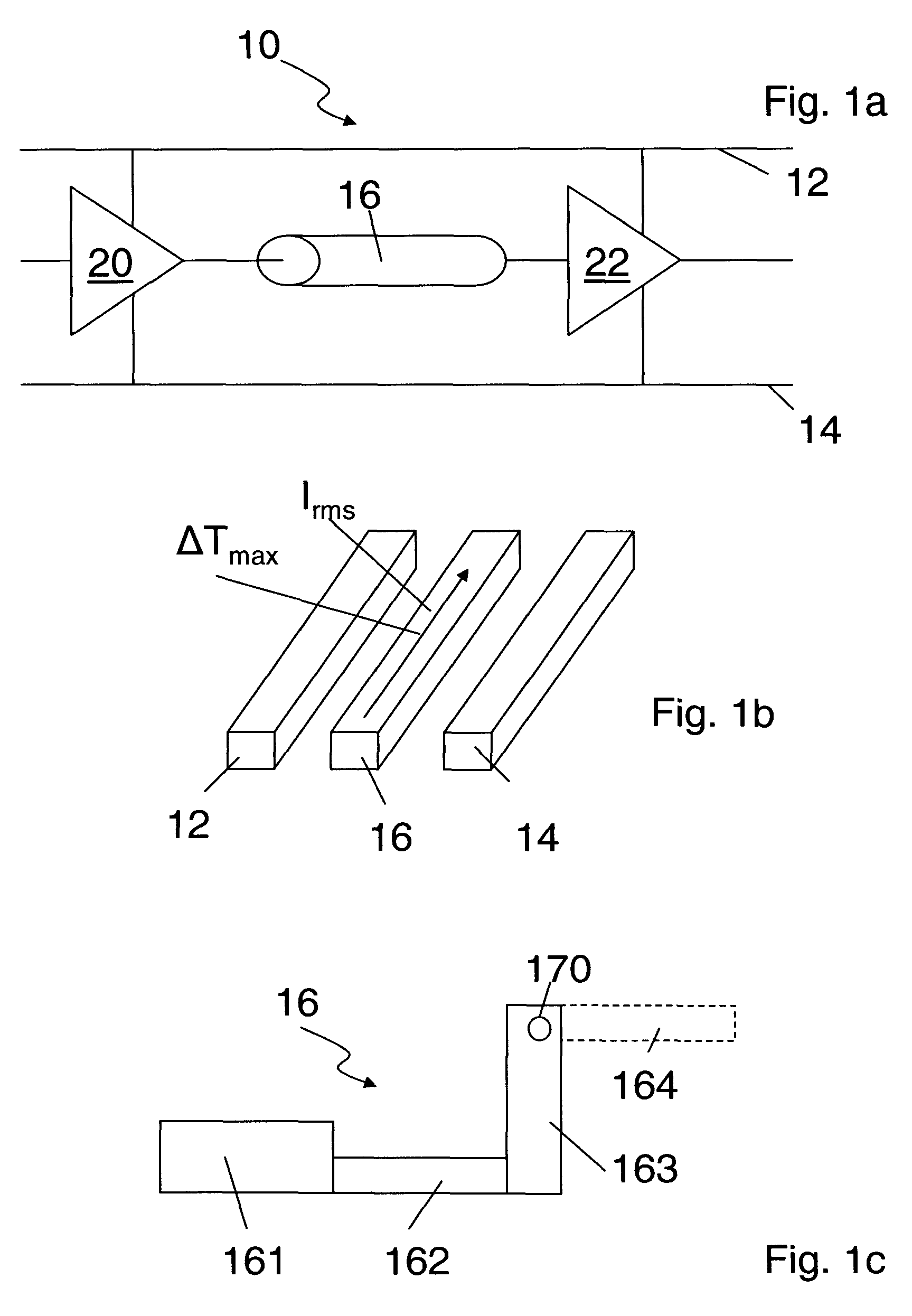
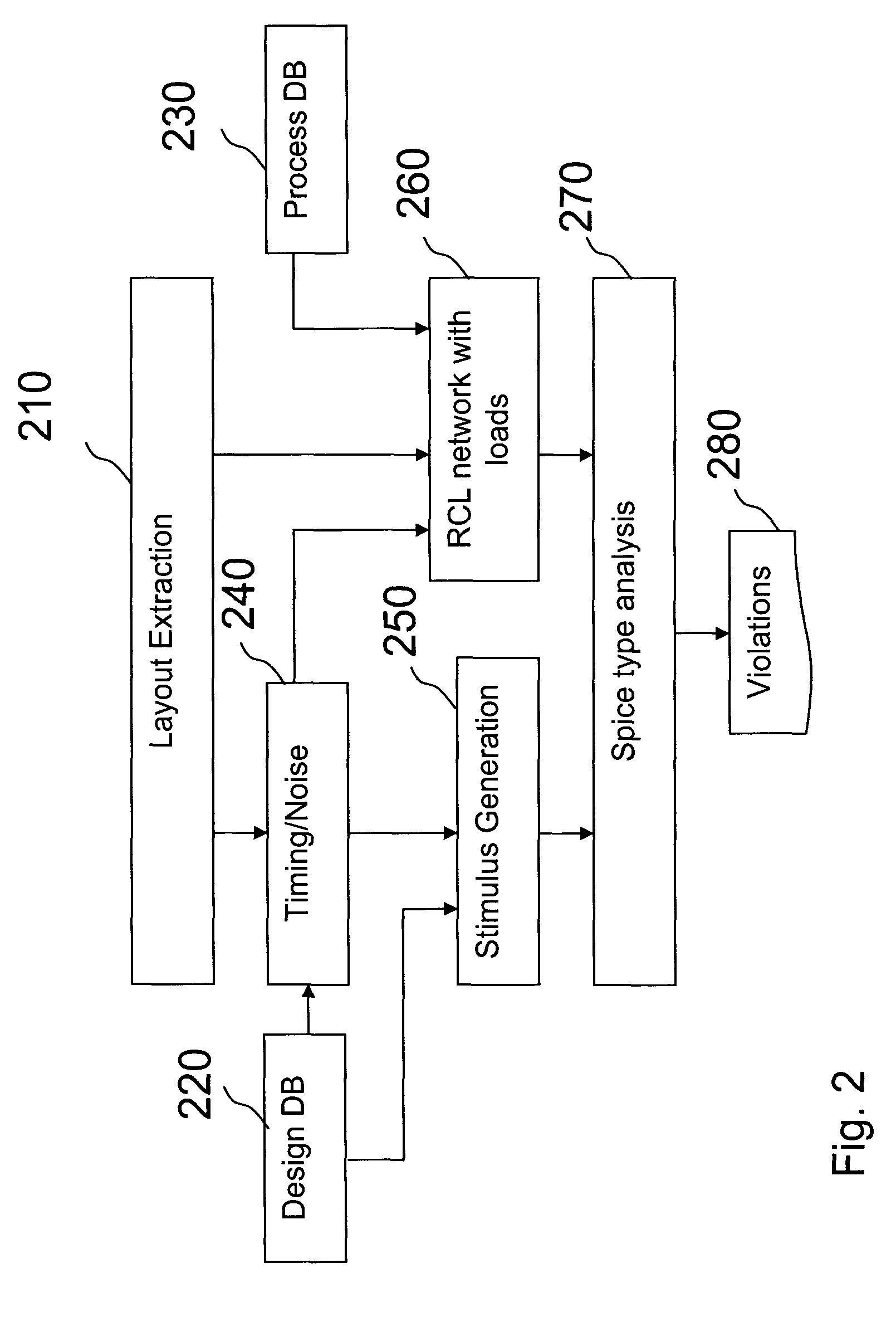
[0041]Generally, the present invention provides a method analyzing probable local failures of wire segments and vias due to electromigration. As the analysis maintains topological information throughout the analysis adjustment of the layout and / or wiring is facilitated and reduced to the areas where adjustment is needed. Local failures can directly be flagged by comparison of readout of the analysis and against annotated maximum limits of effective current and peak current densities.

[0042]Designing a chip with integrated electronic circuits starts out from a netlist which comprises a description of the cells and their intercon...


PUM


Abstract

The invention relates to an electromigration analysis method and a system for analyzing one or more nets in a digital integrated circuit design that are at risk of electromigration. The method comprises the steps of providing at least one interconnect between a driver cell and at least one load cell; applying same extracted netlist data for noise and / or timing analysis and for electromigration analysis; modeling the driver cell by a train of trapezoidal voltage pulses transmitted from the driver cell to the one or more load cells through the at least one interconnect; extracting at least a slew rate of a driver voltage signal and / or timing information from a noise and / or timing analysis for the one or more nets; and comparing a locally measured current density in the at least one interconnect to an effective local maximum current density limit of the at least one interconnect.

Description

FIELD OF THE INVENTION[0001]The invention relates to an electromigration analysis on signal wiring. Specifically, an electromigration analysis method and system are provided which maintain topological information on local electromigration risks.BACKGROUND OF THE INVENTION[0002]Modern integrated circuit designs are becoming more and more complex and compact. Generally, integrated circuits encompass several electronic components such as logic gates, flip-flops, comparators, multiplexers etc. Components in an integrated circuit are interconnected using interconnections such as metal wires, which are also referred to as signal leads or signal wires. A signal wire is typically designed to transfer a signal from a component, known as driver cell, to another component, known as receiver cell or load cell. The signal, when transferred, is characterized by several parameters, particularly current density parameters such as average value, “rms” current densities (rms=root mean square), peak c...

Claims


Application Information

Patent Timeline
Patent Type & Authority Patents(United States)
IPC IPC(8): G06F17/50
CPCG06F17/5036G06F30/367
Inventor KEINERT, JOACHIMSMITH, HOWARD H.WILLIAMS, PATRICK M.
Owner SIEMENS PROD LIFECYCLE MANAGEMENT SOFTWARE INC
Why Eureka
Try Eureka