
Non-volatile memory with guided simulated annealing error correction control

a non-volatile memory and error correction technology, applied in the field of non-volatile memory technology, can solve the problems of erroneous or corrupted data bits, affecting the convergence speed of the data, and the programming state that is sensed can sometimes vary from the intended programming state, so as to achieve fast convergence times and convergence

Active Publication Date: 2011-07-05
SANDISK TECH LLC
View PDF61 Cites 32 Cited by
  • Summary
  • Abstract
  • Description
  • Claims
  • Application Information

AI Technical Summary

Benefits of technology

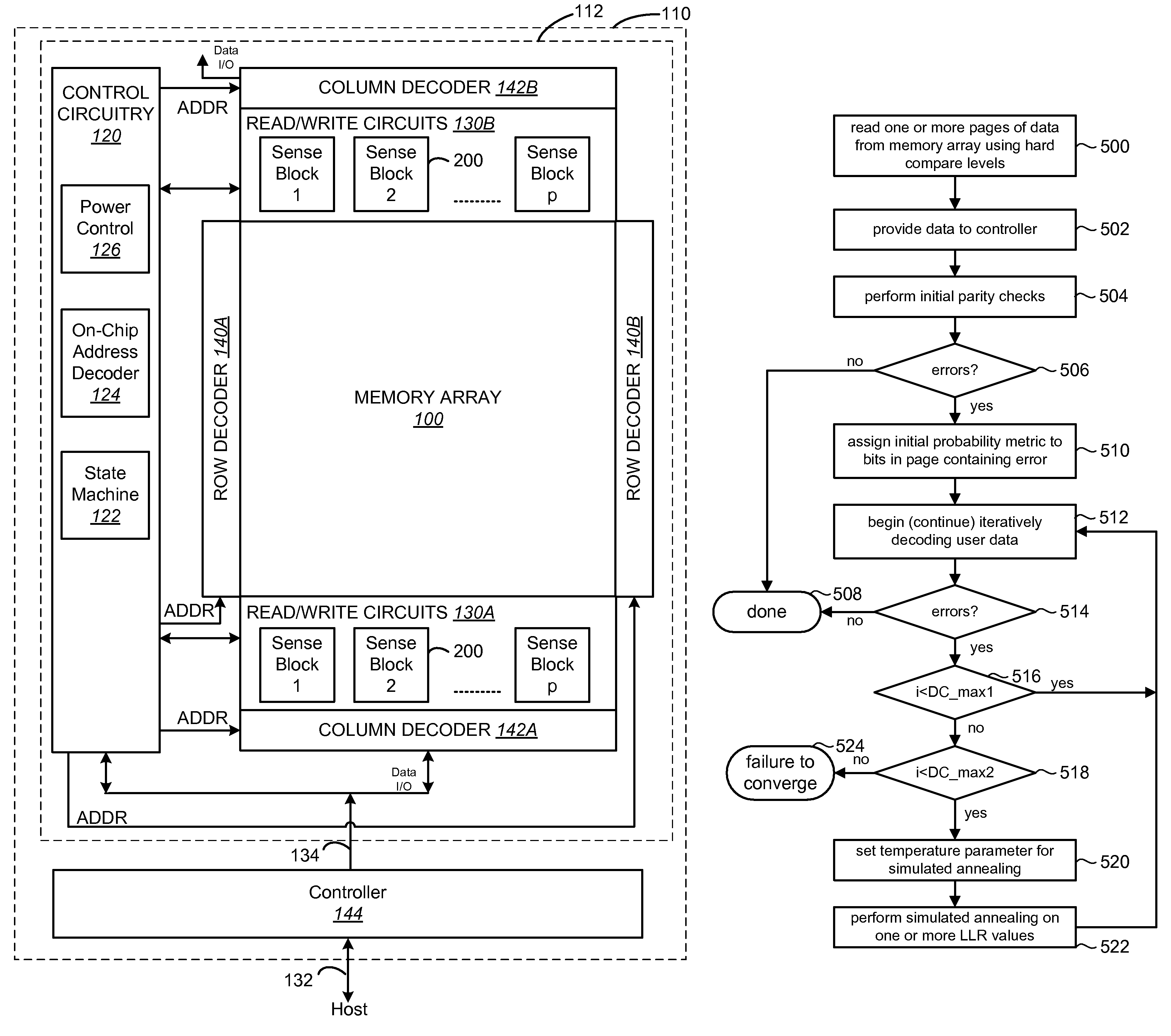
The patent describes a method for decoding data stored in non-volatile storage using iterative probabilistic decoding with error correction codes. The method includes detecting errors in the data, adjusting reliability metrics for bits in code words that represent the data, and simulating annealing to cause a change in the reliability metrics. The method can also include using knowledge of device characteristics to guide the simulated annealing process. The technical effect of the patent is to provide a faster and more flexible method for decoding non-volatile storage, even in situations where data may be uncorrectable.

Problems solved by technology

However, the sensed programming state can sometimes vary from the intended programming state due to factors including noise and the tendency of devices to gravitate towards charge neutrality over time.
Consequently, it is common for to encounter erroneous or corrupted data bits at the time of reading non-volatile memory.

Method used


Image

  • Non-volatile memory with guided simulated annealing error correction control
  • Non-volatile memory with guided simulated annealing error correction control
  • Non-volatile memory with guided simulated annealing error correction control

Examples


Embodiment Construction

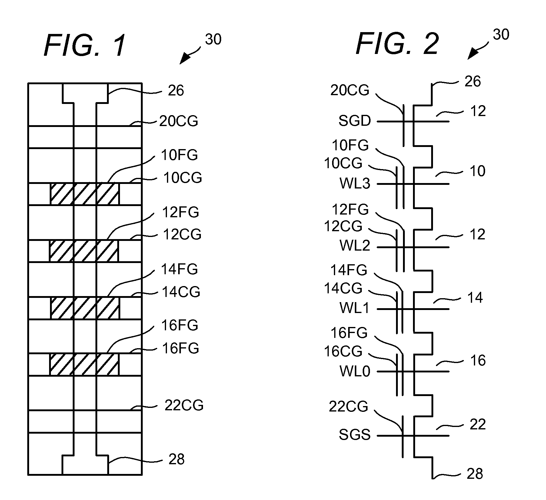
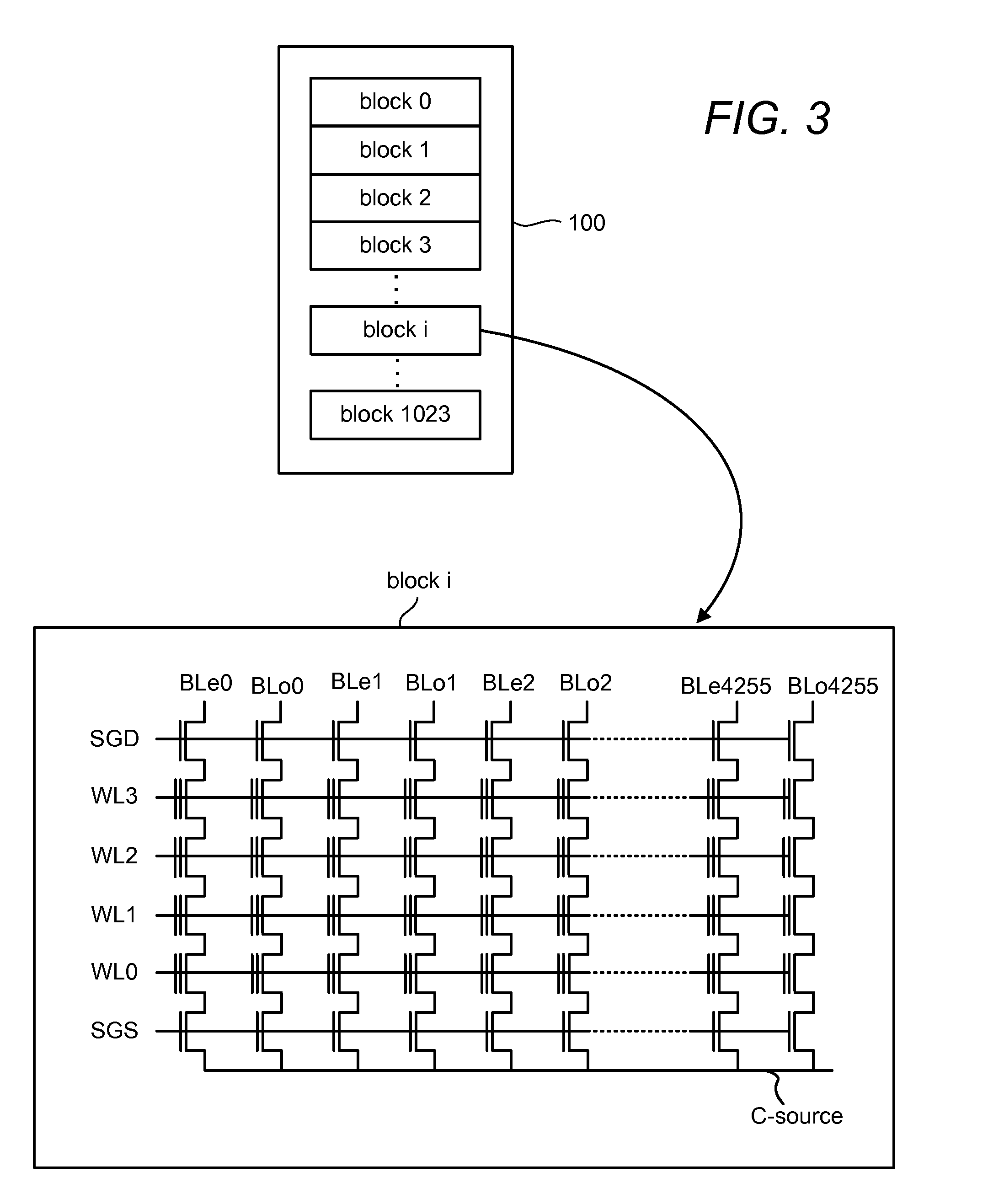
[0033]One example of a flash memory system uses the NAND structure, which includes multiple transistors arranged in series between two select gates. The transistors in series and the select gates are referred to as a NAND string. FIG. 1 is a top view showing one NAND string 30. FIG. 2 is an equivalent circuit thereof. The NAND string depicted in FIGS. 1 and 2 includes four transistors 10, 12, 14 and 16 in series between a first select gate 12 and a second select gate 22. Select gate 12 connects the NAND string to bit line 26. Select gate 22 connects the NAND string to source line 28. Select gate 12 is controlled by applying appropriate voltages to control gate 20CG via selection line SGD. Select gate 22 is controlled by applying the appropriate voltages to control gate 22CG via selection line SGS. Each of the transistors 10, 12, 14 and 16 includes a control gate and a floating gate, forming the gate elements of a memory cell. For example, transistor 10 includes control gate 10CG and...


PUM


Abstract

Data in non-volatile storage is decoded using iterative probabilistic decoding. An error correcting code such as a low density parity check code may be used. In one approach, initial reliability metrics, such as logarithmic likelihood ratios, are used in decoding sensed states of a set of non-volatile storage elements. The decoding attempts to converge by adjusting the reliability metrics for bits in code words which represent the sensed state. Simulated annealing using an adjustable temperature parameter based on a level of error in the data can be performed to. The simulated annealing can introduce randomness, as noise for example, into the decoding process. Moreover, knowledge of the device characteristics can be used to guide the simulated annealing process rather than introducing absolute randomness. The introduction of a degree of randomness adds flexibility that permits possible faster convergence times and convergence in situations where data may otherwise be uncorrectable.

Description

CROSS-REFERENCE TO RELATED APPLICATIONS[0001]This application is related to co-pending, commonly assigned U.S. patent application Ser. No. 11 / 694,951, filed herewith, entitled “Guided Simulated Annealing in Non-Volatile Memory Error Correction Control, ” cross-referenced and incorporated by reference herein in its entirety.BACKGROUND OF THE INVENTION[0002]1. Field of the Invention[0003]Embodiments of the present disclosure are directed to non-volatile memory technology.[0004]2. Description of the Related Art[0005]Semiconductor memory has become increasingly popular for use in various electronic devices. For example, non-volatile semiconductor memory is used in cellular telephones, digital cameras, personal digital assistants, mobile computing devices, non-mobile computing devices and other devices. Electrically Erasable Programmable Read Only Memory (EEPROM) and flash memory are among the most popular non-volatile semiconductor memories. With flash memory, also a type of EEPROM, the...

Claims


Application Information

Patent Timeline
Patent Type & Authority Patents(United States)
IPC IPC(8): H03M13/00
CPCG06F12/0246G06F2212/7209H03M13/1102
Inventor CHIN, HENRYMOKHLESI, NIMA
Owner SANDISK TECH LLC
Learn More