
Real-time background legality verification of pin placement

Active Publication Date: 2011-08-02
ALTERA CORP
View PDF5 Cites 17 Cited by
  • Summary
  • Abstract
  • Description
  • Claims
  • Application Information

AI Technical Summary

Benefits of technology

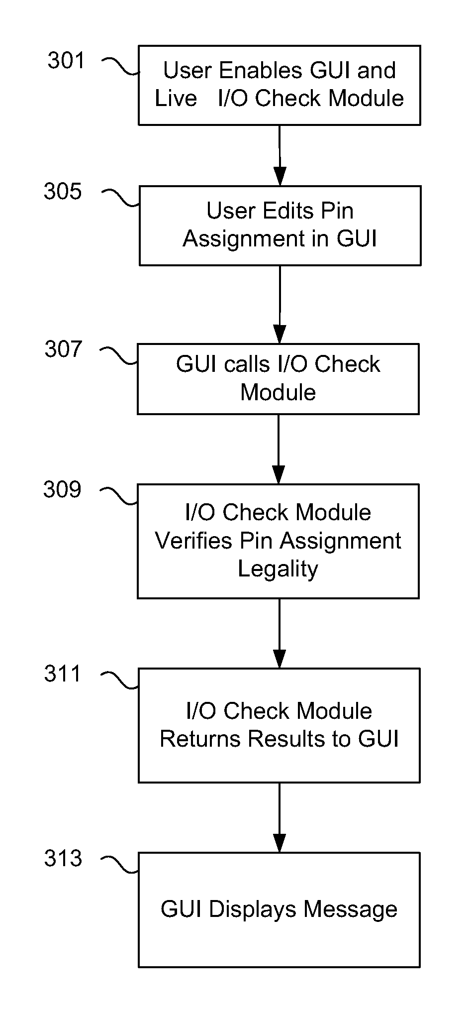
[0005]Programming a PLD requires both logic description design and physical design. A portion of the physical design is input and output (I / O) pin assignments of pin properties that are subject to a number of I / O rules and restrictions. Pin properties to be assigned includes physical locations and electrical properties, e.g., pin position, input / output standard voltage, reference voltage, current density, current strength, input / output direction, slew rate, termination, pre-emphasis, slew rate, toggling rate, bus hold, weak pull-up, and equalization. A legal pin assignment is one that meets the I / O rules and restrictions. The present invention improves the pin assignment and placement process. Pin assignment legality is verified in real-time to reduce the number of input / output assignment analysis runs during physical design of a PLD. The verification process runs on a background thread and preferably on a different processor than the assignment program. Edited pin properties are checked quickly against certain rules, and results displayed to the user usually before a new pin is edited. Available and legal positions are found and displayed for a selected pin.
[0012]One feature of the present invention is a reduction in the time to verify the legality of a pin assignment. Batch processing of pin assignment legality verification often took longer than 3 minutes because all the pins are checked against all the rules. By checking one pin at a time against a subset of rules, e.g., I / O buffer rules only or I / O buffer rules plus some I / O system rules, the legality verification time is dramatically reduced to a few seconds, even for complex designs. For example, a pin assignment legality verification for a medium-sized design takes about 2 or 3 seconds.
[0013]A particular feature of the present invention is to not require a netlist prior to pin assignments. Traditionally, I / O pin assignments occur after all of the logic description design. By distinguishing between I / O buffer rules and I / O system rules, certain rules that do not require a netlist may be checked in real-time as pin assignments are made. Not requiring a netlist means that some physical design can be made before the logic design is complete. Allowing some parallel designing reduces the critical path for the entire system. Of course final verification of the pin assignments including unchecked I / O system rules that require netlist traversal still needs to occur after the logic description design is completed.

Problems solved by technology

Generally, I / O system rules are more complicated than buffer rules and requires status of other pins and components be known.

Method used


Image

  • Real-time background legality verification of pin placement
  • Real-time background legality verification of pin placement
  • Real-time background legality verification of pin placement

Examples


Embodiment Construction

[0023]Reference will now be made in detail to some specific examples of the invention including the best modes contemplated by the inventors for carrying out the invention. Examples of these specific embodiments are illustrated in the accompanying drawings. While the invention is described in conjunction with these specific embodiments, it will be understood that it is not intended to limit the invention to the described embodiments. On the contrary, it is intended to cover alternatives, modifications, and equivalents as may be included within the spirit and scope of the invention as defined by the appended claims.

[0024]For example, the techniques of the present invention will be described in the context of FPGA design, specifically physical design using Quartus II™ from Alterra Corporation of San Jose, Calif. However, it should be noted that the techniques of the present invention can be practiced with other Electronic Design Automation (EDA) tools. In the following description, nu...


PUM


Abstract

Pin placement legality is verified in real-time in a background to reduce a number of input / output assignment analysis runs during a physical design of a programmable logic device. Edited pin properties are checked quickly in the background against certain rules, and results displayed to a user usually before a new pin is edited. Available and legal positions are found and displayed for a selected pin to reduce errors.

Description

FIELD OF THE INVENTION[0001]The present disclosure generally relates to programmable logic devices, and more particularly, to a process of physical design of programmable logic devices.DESCRIPTION OF RELATED ART[0002]A Programmable Logic Device (PLD) is a semiconductor integrated circuit that contains fixed logic circuitry that can be programmed to perform a host of logic functions. In the semiconductor industry, PLDs are becoming increasingly popular for a number of reasons. Due to the advances of chip manufacturing technology, PLDs have improved density and speed performance. Sophisticated programming software enables complex logic functions to be rapidly developed for PLDs. Furthermore, logic designs generally can also be easily migrated from one generation of PLDs to the next, further reducing product development times. The closing of the price-performance gap with Application-Specific Integrated Chips (ASICs) and reduced product development times makes the use of PLDs compellin...

Claims


Application Information

Patent Timeline
IPC IPC(8): G06F17/50
CPCG06F17/5054G06F30/34
Inventor IOTOV, MIHAILPATEL, KAMALWENZLER, MICHAEL V.
Owner ALTERA CORP
Learn More