Flexible OLED display with chiplets

a technology of oled display and chiplet, which is applied in the manufacture of electrode systems, discharge tubes/lamps, and discharge tubes/lamps, etc., can solve the problems of non-uniform electrical performance and visual appearance of displays employing such materials, low performance of thin-film transistors made of organic materials (otfts), and less electrical performance of display devices. achieve the effect of improving flexibility, improving electrical performance and simplifying structur

Active Publication Date: 2011-09-06
GLOBAL OLED TECH
View PDF13 Cites 9 Cited by
  • Summary
  • Abstract
  • Description
  • Claims
  • Application Information

AI Technical Summary

Benefits of technology

[0019]The present invention provides a simplified structure for a flexible light-emitting diode device with higher performance and improved flexibility. This invention permits the use of a substrate having a rough surface that reduces the need for substrate processing to provide a smooth substrate surface, thereby reducing manufacturing process requirements and enabling the use of a wider variety materials.

Problems solved by technology

Thin-film transistors (TFTs) made from amorphous or polycrystalline silicon are relatively large and have lower performance compared to conventional transistors made in crystalline silicon wafers.
Moreover, such thin-film devices are formed at high temperatures (e.g. >300° C. for amorphous silicon and >500° C. for large-grain polysilicon) and typically exhibit local or large-area non-uniformity across the glass substrate that results in non-uniformity in the electrical performance and visual appearance of displays employing such materials.
Thin-film transistors made of organic materials (OTFTs) have lower performance than silicon TFTs and are more susceptible to moisture but are processed at lower temperatures (e.g. <200° C.)
Flexible substrates made of plastic are relatively transparent but have many limitations.
Such substrates typically physically degrade at temperatures greater than 300° C. or even at 250° C. or 200° C. Hence processing the substrate, or materials deposited on the substrate, is very difficult.
For example, conventional PEN has a process temperature of approximately 150° C. and PET has a process temperature of approximately 120° C. Furthermore, plastics can have limited resistance to chemicals and processes used in conventional photolithography, thereby limiting the kinds of materials and processing employed with the substrates.
Such substrates are also know to have poor dimensional stability with varying process temperatures, stress, and relative humidity, thereby limiting the resolution of structures formed on the substrate.
Moreover, as noted in U.S. Pat. No. 7,466,390, it is difficult to form plastics that are smooth and clean enough to serve as a substrate for the formation of thin-film electronic elements, such as those commonly used for flat-panel displays, e.g. thin-film silicon transistors.
Catalytic byproducts and inorganic particulates in the polymers and inadequate process conditions all affect surface roughness.
For soft materials such as polymers, artifacts such as scratches or foreign contaminants can be problematic.
Such products, however, are still relatively rough, face many of the difficulties listed above, and are inadequate for thin-film display devices using thin-film transistors without additional stabilization and surface treatments.
Metal foils have the advantages of moisture impermeability, a lower coefficient of thermal expansion, and are relatively inexpensive as well as compatible with high process temperatures of, for example 900° C. Metal foils, for example steel or aluminum foil, however, are opaque and thus cannot serve as both a substrate and cover in a flat-panel display device (since light must escape from a flat-panel display).
However, such smoothing processes are expensive and time consuming.
Moreover, the costs of the substrates increase if additional treatments to stabilize the substrate materials are necessary.
However, these substrates are relatively thick and not well adapted to flexible devices.

Method used


Image

  • Flexible OLED display with chiplets
  • Flexible OLED display with chiplets
  • Flexible OLED display with chiplets

Examples


Embodiment Construction

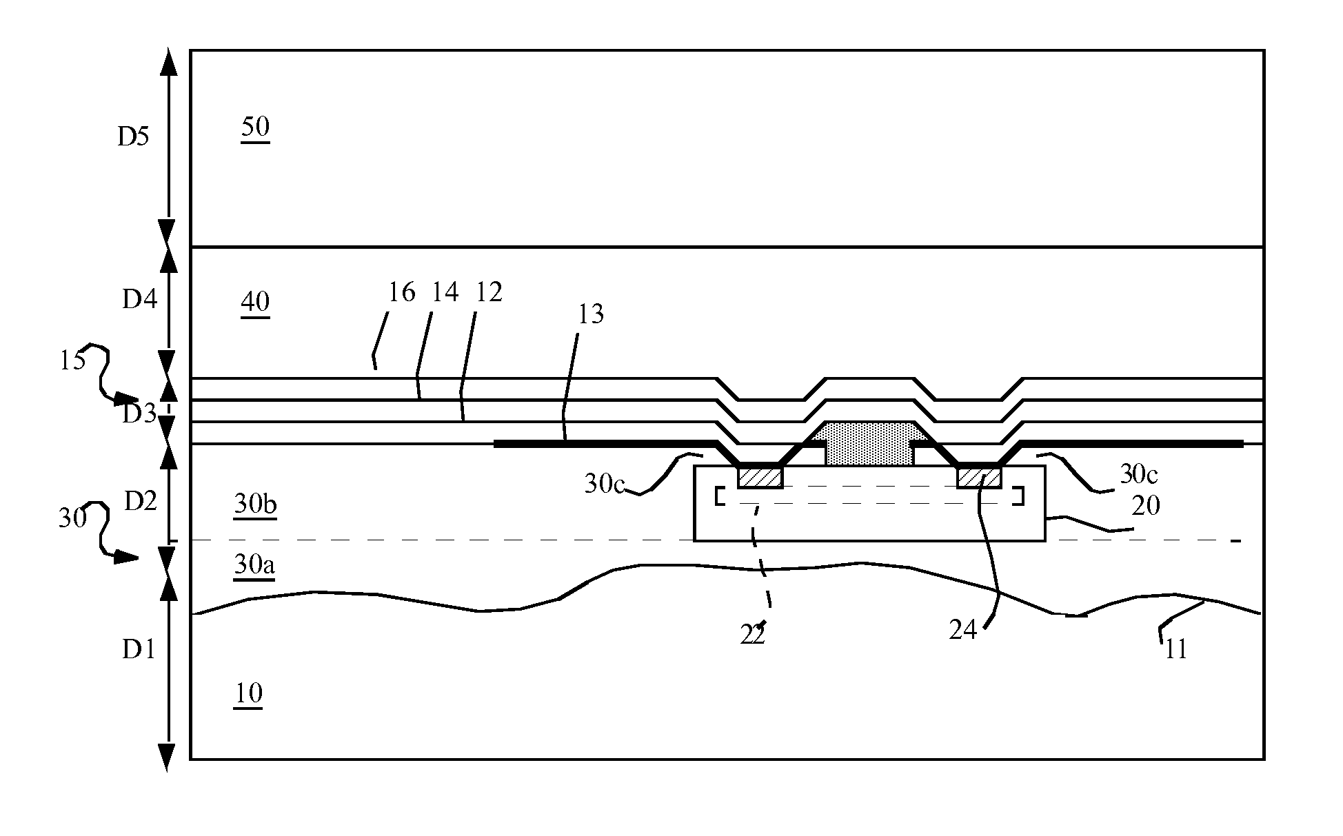
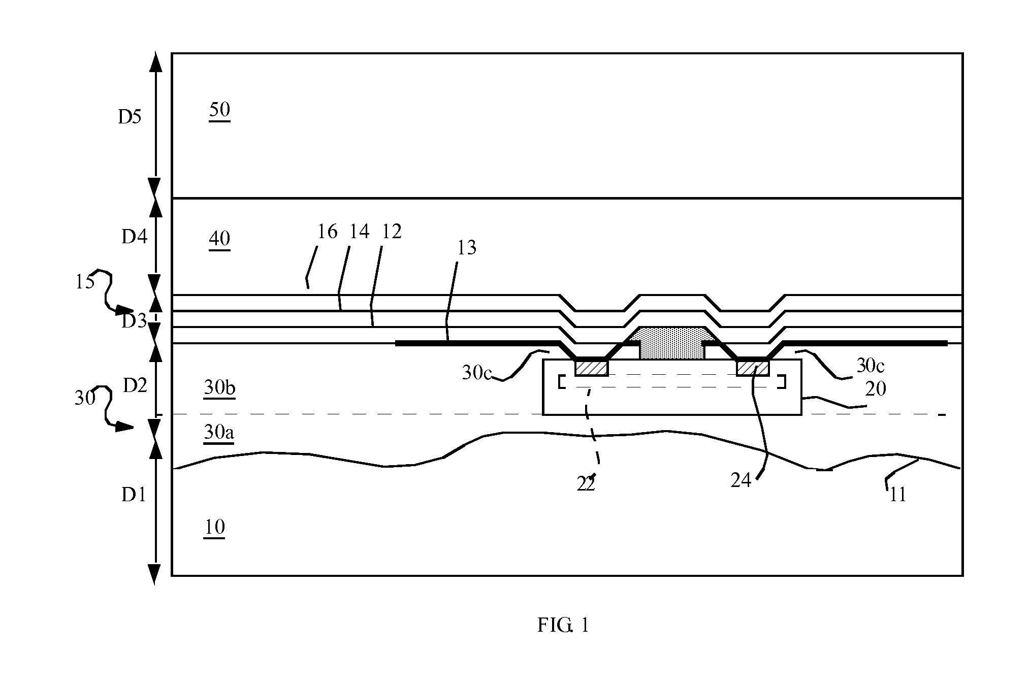
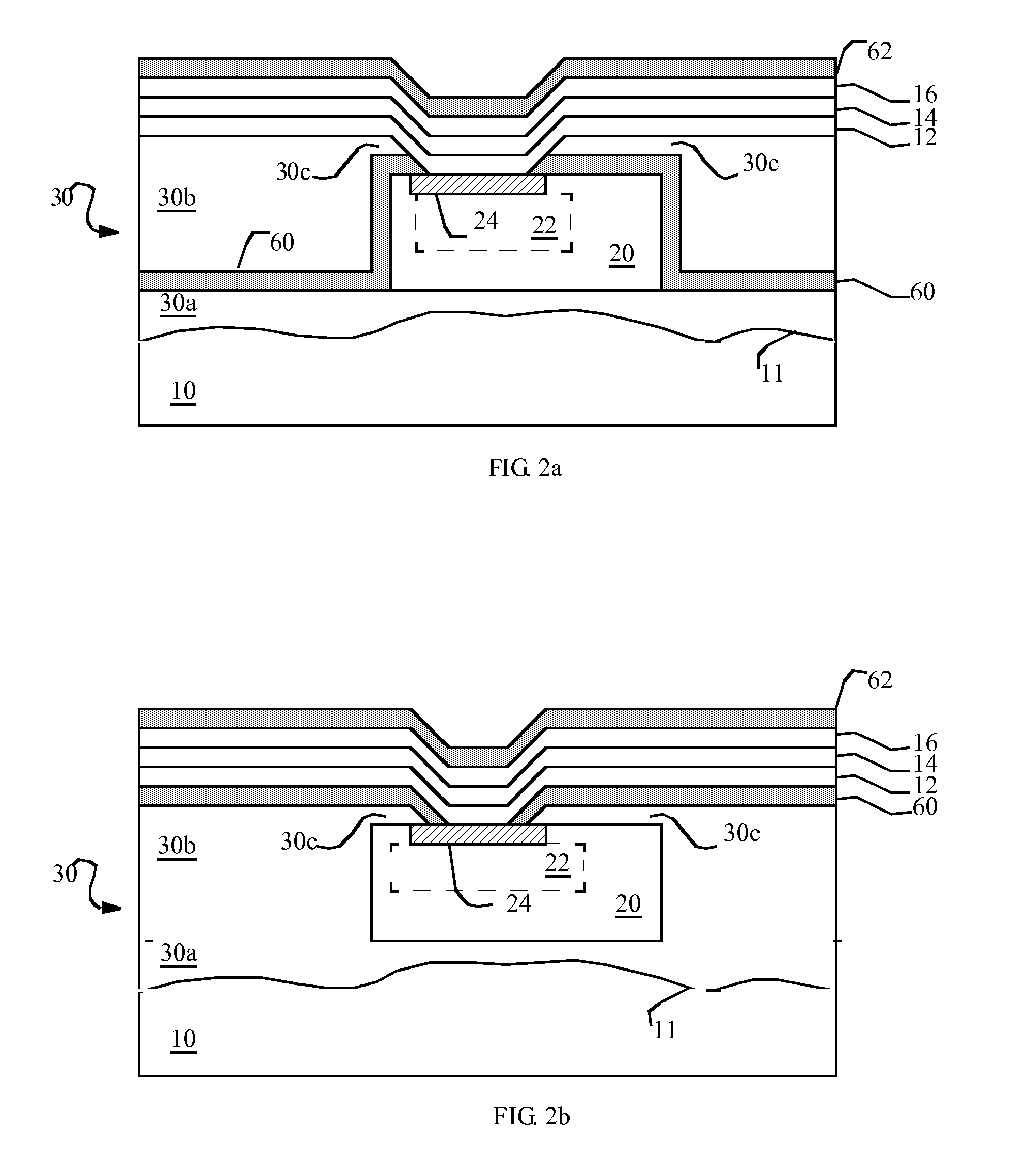
[0024]Referring to FIG. 1, a flexible emissive device 1 includes a flexible rough substrate 10 having a rough substrate surface 11. A display area 21 is defined over the flexible rough substrate 10 (FIG. 3). An organic low-temperature adhesion layer 30 is formed on the rough substrate surface 11, at least a portion of the organic low-temperature adhesion layer 30 having a thickness D2 greater than or equal to 5 microns. A plurality of chiplets 20 are adhered to the rough substrate surface 11, each chiplet 20 having one or more connection pads 24 and the plurality of chiplets 20 distributed in the display area 21. A plurality of patterned bottom electrodes 12 are formed over the organic low-temperature adhesion layer 30 in the display area 21, each bottom electrode 12 is electrically connected to a connection pad 24 of one chiplet 20. One or more layers 14 of light-emitting material are formed over the bottom electrode 12 and a top electrode 16 is formed over the one or more layers 1...


PUM


Abstract

A flexible emissive device, includes a flexible rough substrate having a rough substrate surface and defining a display area; an organic low-temperature adhesion layer formed on the rough substrate surface, at least a portion of the organic low-temperature adhesion layer having a thickness greater than or equal to five microns; a plurality of chiplets distributed in the display area and adhering to the organic low-temperature adhesion layer, each chiplet having one or more connection pads; a plurality of patterned bottom electrodes formed over the organic low-temperature adhesion layer in the display area, each bottom electrode being electrically connected to only one connection pad of a corresponding chiplet; one or more layers of light-emitting material formed over the bottom electrode; and a top electrode formed over the one or more layers of light-emitting material; and a flexible encapsulating layer located over the top electrode and adhered to the rough substrate surface.

Description

CROSS REFERENCE TO RELATED APPLICATIONS[0001]Reference is made to commonly-assigned, U.S. patent application Ser. No. 12 / 191,462, filed Aug. 14, 2008, entitled “Display Device With Chiplets” by Cok et al; U.S. patent application Ser. No. 12 / 271,952 filed Nov. 17, 2008 entitled “Emissive Device With Chiplets” by Cok et al and U.S. patent application Ser. No. 12 / 369,163 filed Feb. 11, 2009, entitled “Display Device With Chiplets and Light Shields” by Cok et al, the disclosures of which are incorporated herein.FIELD OF THE INVENTION[0002]The present invention relates to a flexible light-emitting device employing independent control elements having separate substrates distributed over a flexible rough substrate.BACKGROUND OF THE INVENTION[0003]Flat-panel display devices are widely used in conjunction with computing devices, in portable devices, and for entertainment devices such as televisions. Such displays typically employ a plurality of pixels distributed over a substrate to display ...

Claims


Application Information

Patent Timeline
Patent Type & Authority Patents(United States)
IPC IPC(8): H01J1/62H01J63/04
CPCH01L27/3255H01L27/3276H01L2224/95092H01L2251/5338H01L2924/12044H10K59/129H10K59/131H10K2102/311H01L2924/00H10K10/46
Inventor COK, RONALD S.HAMER, JOHN W.
Owner GLOBAL OLED TECH
Why Eureka
Try Eureka